
How Copper Foil Roughness Affects Impedance and Losses
If you look at the RLGC model for transmission line impedance, you’ll see four parameters that contribute to impedance (all are in their standard units per unit length):
- R: DC resistance of the transmission line, which depends on the line’s conductivity;
- L: loop inductance of the transmission line, taken purely as a function of the line geometry;
- C: total capacitance of the line, also taken as a function of the line geometry;
- G: conductance of the substrate, meant to model the loss tangent at a specific frequency and any parasitic DC conductance.

One thing that many in the industry will not tell you is this: all these parameters are frequency-dependent, including the resistance term! You’re probably thinking “wait a minute, everyone in my EE101 classes said resistance does not depend on frequency. What gives?”
I believe it was back in 2014 when the IEEE P802.3bj Task Force was first presented with a proposal to accept a causal model for 100 Gb/s Ethernet PHY interconnects. In this model, the inductance, capacitance, and resistance terms above were modified to include frequency dependence. The capacitance term was modified easily by accounting for dispersion in the substrate. What about the resistance and inductance? This dependence of resistance on frequency arises due to the skin effect in a conductor at high frequencies.
The skin effect refers to a confinement of current near the surface of a conductor when the current oscillates at high frequency. For a perfectly smooth conductor, the skin effect is marginal until you get up to GHz frequencies. However, in the presence of copper roughness, losses can become considerable within a certain range of frequencies. The skin effect also increases the inductance of the line. The overall effect is a modification in the line impedance from the value predicted in the standard RLGC model.
Even if you do not consider dispersion in the substrate, dispersion in the equivalent circuit terms will always cause a deviation from the ideal impedance. Once you get deep into the microwave and mmWave regimes, you are forced to account for copper roughness when designing an interconnect.

Modeling Copper Foil Roughness and Causality
Modeling copper foil roughness doesn’t require an integrated electromagnetic field solver. Don’t get me wrong, this will probably give you the most accurate results, but it would definitely be considered overkill. Instead, your design software only needs to include a roughness correction factor in an accepted causal PCB transmission line model. When we say “causal,” we are referring to the type of behavior in which a signal response is not seen until after a driver sends a signal down an interconnect. While this may sound obvious, causality violations in high speed/high frequency signal models are common.
So why do causality violations occur in PCB interconnect models? For that matter, why do they occur in any other model? This results from incorrect modeling of the relationships between various physical properties. Regarding electronics, if you accept that causality is the correct description of reality, then you can construct relationships between the physical properties of a PCB substrate and conductors using Kramers-Kronig relations for the real and imaginary parts of a physical property.
If you’re familiar with dispersion in FR4 and other PCB substrates, then you should know about the wideband Debye model or Lorentzian model for describing dispersion. This model is actually derived from the Kramers-Kronig relations between the real and imaginary parts of the substrate dielectric constant:

If you know the real part of the dielectric constant at a range of frequencies, then you can calculate the imaginary part, and vice versa. This same technique is applied to copper foil roughness in a PCB. This can get quite mathematically intense and has formed a part of my own research on transmission line optimization.
The result is this exercise is that the dielectric constant of a laminate clad with rough copper is marginally increased from the base material value. This is not necessarily accounted for in reported Dk values on a datasheet; those are extracted from multiple measurements and will apply to any of a vendor's laminates in a product line, regardless of roughness. If you know the roughness parameters, you can calculate them using the well-known result from Bert Simonovich:

Accounting for Copper Foil Roughness in Your PCB Layout
In the old days, you would have to account for copper roughness manually when designing an interconnect. In other words, you might have to manually account for a roughness correction factor, and then manually add this into the standard RLGC impedance equation. Two standard models for including roughness in interconnect impedance calculations are the Hammerstead model and the Cannonball-Huray model, although there are others. The latter model accounts for roughness in the SEM image below as a snowball or cannonball arrangement.
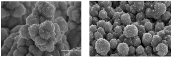
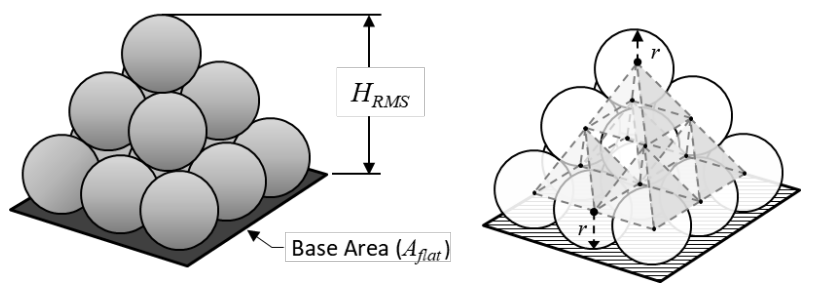
Based upon this geometry and model, you would then apply a causal roughness correction factor to the skin resistance in the above impedance equation. This is easily defined as follows with a functional transformation:

In other words, just replace the skin resistance with the value listed in this expression.
Now all that is left is to determine the value of K. The Cannonball-Huray model provides this definition, as does the Hammerstad model. The values of K in these models will be functions of frequency, dimensions of the copper particulates, the DC conductivity of the copper film, and the roughness as measured with a profilometer or atomic force microscope (AFM).
I would argue, as have others working on copper roughness, that the best approach is to use tabulated process-specific data to define the roughness function K. This would be done by using a series of skin resistance measurements through comparison with a theoretically smooth conductor, something which is beyond the scope of this article and would be adopted by a fabricator. Assuming you can get that kind of numerical data at successive frequency values, you can then use that in the above equation to calculate the real skin resistance at any frequency.
How are Copper Roughness and Impedance Correlated in Practice?
Once you have an expression for the impedance profile, we have to ask, how does this affect signal propagation? This would be visualized using S-parameters. For a given interconnect, we can clearly see differences in loss behavior in the return loss and insertion loss spectra when rough and smooth lines are compared. You could measure these directly, or assuming you had the impedance function, you could calculate the S-parameters using input impedances and attenuation values. I prefer to use ABCD-parameters as they are very easy to work with in transmission lines.
The example below shows some simulated S-parameters I've generated and presented in my IEEE and EDICON seminars. The differences in return loss and insertion loss are clearly visible, even though these lines would nominally perform near 50 Ohms within tolerances for any signaling standard.

Do these differences matter? The answer is: it depends on the length of the interconnect and frequency. At lower frequencies, the differences are less pronounced, so they matter less. The length of the interconnect also matters. If the interconnect is long, losses will be dominated by insertion loss, which will create greater loss differences at higher frequencies (note the dB/in. units in the above graph). In shorter interconnects, the return loss will dominate signal behavior, both at the input of the transmission line and at the output. This also matters more at higher frequencies because, eventually, the load capacitance takes over and there will be significant reflections off the load, even if broadband termination is applied properly.