
Clearly, the need to accommodate fine pitch components or simply a higher density of components is what motivates the need for HDI designs. Traces are fabricated in the same manner as traces on any other PCB, although care is taken to prevent over-etching. Vias are a different beast and may require laser drilling (for low aspect ratios) through a single layer, known as blind or buried vias.
If you need to span multiple layers in an HDI PCB board, you can’t use a through-hole via anymore and still comply with IPC standards. For larger diameter microvias, some manufacturers have experience fabricating blind vias that span multiple layers, but this is not common. Furthermore, placing this in your design will likely violate your manufacturer’s DFM rules and will cause your board to receive no-bid status. Instead, vias can be placed in individual layers and stacked on top of each other (e.g., stacked micro vias or blind-buried vias). The various microvia configurations are shown below.
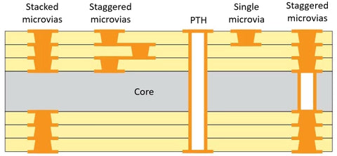
Microvia configurations in a typical HDI layout.
These different configurations are primarily targeted at BGA components with different pitches. Once your BGA pitch gets to 0.8 mm, you’ll likely be able to use a dog bone fanout with in-pad micro vias. At 0.75 mm and less, you’re better off using plated in-pad microvias (VIPPO) to reach inner signal layers, although you can also route signals between BGA pads to reach the outer pad section during fanout. At a much lower pitch (e.g., 0.5 mm), it is not recommended to route between pads unless your manufacturer can reliably fabricate traces below 4 mils.
Basic HDI Design Guidelines
When working with fine-pitch BGA, and the traces and vias that connect to it, there are some basic guidelines that apply to any HDI layout.
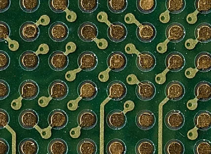
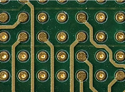
Two HDI layout examples with BGAs. Top: Dogbone fanout with microvias. Bottom: Microvia in-pad.
- Always check your manufacturer’s capabilities. You should generally do this anyways before planning a new design, but nowhere else is this more important than in HDI PCB design. Not all manufacturers have the same capabilities in this area, and it’s best to check with your desired manufacturer before you create an HDI layout that can’t be fabricated.
- Keep track of spacing between traces and pads. The same idea applies in 1 mm pitch BGAs, the only point that changes are scaling to micro via sizes. Solder mask clearance values are typically the same size as your trace width. The solder mask clearance depends on the pad size and your pad pitch.
- Don’t use staggered vias or ELIC if you don’t need them. The whole point of HDI routing is to provide as much space as possible for routing on the surface and inner layers. While it might be tempting to stack across the entire span of the substrate, don’t take up the extra space unless it’s really necessary.
- Opt for fewer layers. High layer count boards bring more assembly steps and manufacturing costs. If you follow the previous guideline, you can significantly reduce the cost per board.
- Don’t forget about signal integrity when working with HDI boards. Any HDI layout will need to be designed with high-speed design guidelines in mind, or high-frequency guidelines if you’re working with an RF board. The same signal integrity rules that apply in typical PCBs still apply in HDI PCBs, it’s just a matter of scaling. In an HDI board that requires impedance-controlled routing, you’ll need to carefully design your traces and stack up to ensure your impedance is consistent with your signaling standard.