
STACKUP DESIGN AFFECTS SIGNAL INTEGRITY
As stackup design affects signal integrity, designers must consider PCB stack up design as one of the most important aspects of their initial design activity. The main reason is fabrication processes for PCBs are not exact enough to match the material choices, trace widths, dielectric, and copper thicknesses you may have carefully defined. Moreover, vendors usually have different equipment and methods.
The fabricator may have to change the materials if they are not readily available or in stock. A reliable vendor would need to make the proper combination and in-process adjustments so that tolerances that add up in all areas work towards fulfilling your specifications, especially when measuring impedances on the test coupon. To fulfill your impedance requirements, your vendor may have to make small changes to the material thickness and trace widths.
PREFERENCE FOR HDI LAYER STACKUP
For boards with several high pin-count BGAs, you could have PCBs using standard lamination with through vias, sequential lamination with blind and buried vias, or a PCB stackup with micro-vias. Although the first type offers several advantages such as low cost, simple via models, and high reliability with a familiar and mature fabrication process, it is unfortunately limited to a low layer count. The simpler fabrication process also tends to make vias large in diameter, reducing the routing ability, and forcing the designer to increase the number of layers.
The second type of stackup using sequential lamination with blind and buried vias, generally has simple vias with a lower aspect ratio, allowing smaller hole sizes. Although this improves the routing ability, the process still does not allow reducing trace widths, resulting in only a few fabricators adopting the process, the most preferring the HDI PCB process instead.
The third type of stackup using micro-vias is the HDI PCB technology, where fabricators use laser beams to form very small diameter vias also known as micro-vias. As a result, this technology also allows very small features for both vias and traces, enabling very high routing density and fewer layers. Designers can stack or stagger micro-vias and apart from opening up routing channels, this is the only practical way so far available for designing with multiple large BGAs of 0.8 mm or lower pitch.
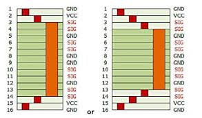
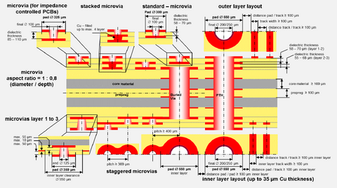
Fig. 2: HDI Stackup IPC Type III
Appropriate PCB stackup design with HDI technology not only improves signal and power integrity, it provides the lowest cost for high-density boards. Materials used in HDI technology ate more suitable for use in processes requiring lead-free soldering and RoHS.
At present, most handheld and consumer electronics manufacturers prefer the HDI technology, as this gives the best alternative to high layer-count sequentially laminated or expensive standard laminate boards. This is especially true as the trend is more towards finer pitch and higher pin-count components such as BGAs, LQFPs, and CSPs.
The Institute of Printed Circuits (IPC) in collaboration with the Japan Printed Circuits Association provides standards such as IPC/JPCA-2315, which offer easy tutorials on HDI and micro-via design rules and their structures. It also offers advice on selection of materials, considerations when designing an High-Density Interconnect PCB, while providing design examples and processes for various micro-via technologies.
ALSO READ: DIFFERENT STACKUPS FOR HDI PCBS
STACKUP DESIGN STANDARD
HDI PCB stackup design may follow six types as the IPC-2315 standard specifies. Of these types IV, V, and VI are of the expensive type for fabrication, and not suitable for large dense PCBs.
HDI PCB stackup design IPC Types I and II use a laminated core, micro-vias, buried vias, and through vias. However, as they use a single micro-via layer on at least one side, it makes these types unsuitable for fabricating large, dense boards.
HDI PCB STACKUP DESIGN IPC TYPE III
Since HDI PCB stackup design IPC Type III allows use of two or more micro-via layers on at least one side of the board, this is the most suitable for large, dense boards with multiple high pin-count BGAs. In an IPC Type III stackup, fabricators can drill via holes in the laminated core, and the via become buried as they add dielectric material for the micro-via layers. Designers may stagger or stack micro-vias in relation to themselves and other buried vias in the PCB.
In the IPC Type III PCB stackup design, designers can use the outer layers as GND planes, thereby improving EMI/EMC requirements. In such cases, designers can use the inner layers for placing Power planes and micro-vias for signal routing. While this may not be feasible in a 4-layer PCB stackup design, the strategy works very well for 8-layer PCB stackup, 10-layer PCB stackup, 12-layer PCB stackup, and higher.
The designer decides on the number of cores and the buildup layers actually required for a specific board. The final PCB stackup design depends on the designer’s management of the plane layers, routing density, and signal integrity requirements.
For instance, the designer may improve routing density by removing all unused pads on buried vias. This also reduces crosstalk significantly. Similarly, keeping via aspect ratios to 5:1 for micro-vias, 10:1 for buried vias, and micro-via pad sizes to about 0.15 mm larger than the hole, helps to improve the routing density largely.
While stacking vias offers the most flexibility and efficiency to a designer for routing a multi-layer board, it is a more expensive process compared to the process of using staggered vias. Moreover, if the designer has used buried vias, he/she can easily extend the buried via into the first micro-via layer, as this will take up less space, for say, extending ground and power nets all the way through the board. However, the fabricator may charge more for extending buried-vias rather than having them in the laminated core alone.
IMPROVING ROUTING ABILITY IN HDI PCB IPC TYPE III
Designers use several techniques for improving routing ability in their boards to reduce the number of layers effectively. As large dense boards often use fine-pitch BGAs, the location of vias with respect to the BGA pads assumes greater significance for improving the routing ability. For instance, designers may place vias adjacent to the BGA pads, causing dog-bone type structures. For even greater density, designers may prefer to use via-in-pad design, offset via-in-pad design, or partial via-in-pad design, of which, the first offers the greatest opportunity for increasing the routing density. Ultimately, improving the routing density reduces the layer count and hence, the overall fabrication costs.
ALSO READ: WHY YOU NEED AN HDI PCB?
IMPROVING POWER INTEGRITY IN HDI PCB IPC TYPE III
HDI stackup in IPC Type III boards affects the power and signal integrity depending on how the designer locates the power and ground planes. For instance, a designer may decide to assign the GND plane to the outermost layers, as this provides an excellent EMI shield. Additionally, the designer may assign GND to the outermost layers and VCC to the adjacent layers.
Apart from the advantages of an EMI shield, this strategy improves the capacity coupling between the GND and Power layers, resulting in minimizing bypass capacitors a BGA needs. This strategy also allows an opportunity to the designer for using embedded pull-up resistors and bypass capacitors, while opening up additional routing space on all signal layers. Moreover, stripline configurations with pairs of signal layers sandwiched between plane layers reduce crosstalk drastically, while providing the best return paths.
Designers can use split planes or even dedicated voltage layers for distributing powers to large BGA requiring multiple voltage supplies. They can improve the power integrity by placing a couple of voltage supply layers near the center of the board, and surround it with GND planes. This way, designers can avoid the splits or different voltages affecting signal layers that cross them.
CONCLUSION
The best HDI layer stackup design depends on the priorities of the designer. It is best to analyze each stackup for relative cost, routing density, power density, signal integrity, and power integrity. Large dense PCBs benefit from HDI stackup using IPC Type III PCB stackup design, where the outermost layers are the GND and Power layers, with micro-vias in at least two inner layers on at least one side for maximizing routing density.