Basic Structure of FPGA
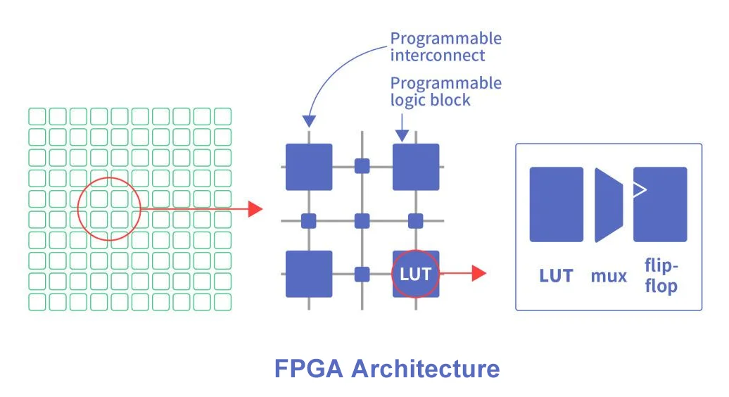
The FPGA architecture mainly includes four parts: configurable logic block (CLB), input and output block (IOB), internal wiring (Interconnect) and other embedded units. The internal structure of the FPGA device is shown below.

Configurable Logic Block (CLB)
CLB is the basic logic unit of FPGA. The actual number and characteristics will vary from device to device, but each CLB contains a configurable switch matrix of 4 or 6 inputs, several selection circuits (multiplexers, etc.), and flip-flops.
Input and Output Block (IOB)
FPGAs can support many I/O standards, making them an ideal interface bridge for system designs. The I/O in the FPGA is grouped by bank, and each bank can independently support different I/O standards. At present, the most advanced FPGA provides more than ten I/O banks, which can provide flexible I/O support.
Internal Wiring (Interconnect)
The CLBs provide the logic performance, and the flexible interconnect routing is responsible for passing the signals between the CLBs and the I/Os. There are several types of routing, ranging from dedicated CLB interconnects (short wire resources), to high-speed horizontal and vertical long wires (long wire resources) within the device, to global low skew routing for clocks and other global signals (global dedicated routing resources).
Embedded Units
Embedded hard core units include RAM, DSP, DCM (Digital Clock Management Module) and other specific interface hard cores, etc.
FPGA Features
- Using FPGA to design ASIC circuit, the cycle is short, the cost is low, the risk is small, and the quality is stable;
- FPGA adopts high-speed CHMOS technology with low power consumption;
- FPGA architecture, flexible logic unit, high integration, wide application range;
- FPGA is compatible with the advantages of PLD and general gate array, and can realize large-scale circuits;
- On-site reprogramming is possible, and the later maintenance cost is low;
- FPGA is a parallel computing that can meet multi-functional requirements at the same time.
How does FPGA Work?
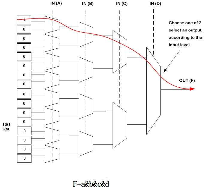
FPGA implements logic functions by loading programming data to internal static storage units. The value stored in the storage unit determines the logic function of the logic unit and the connection mode between each logic unit module or between the module and I/O, and finally determines the FPGA The function realized. FPGA uses a small look-up table to implement combinational logic, each look-up table is connected to the input of a D flip-flop, and the D flip-flop is used to drive other logic circuits or I/O, thus forming a combined logic function and realizing The basic logic unit module of the sequential logic function, these modules are connected to each other or to the I/O module by metal wires.
Here’s an simple example to explain the principle of the FPGA:

As shown in the figure above, we configure 16bitRAM as 0000000000000001, and this circuit is equivalent to F=A&B&C&D;
Only when A=B=C=D=1, F=1, otherwise F=0;
“0000000000000001” This string of numbers is FPGA programming.
Logic Block of FPGA
There is a proper term in FPGA, called LUT, lookup table (lookup table).
The LUT constitutes the most basic unit of any FPGA.
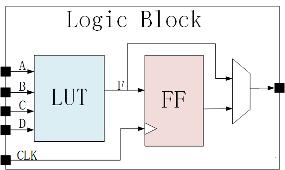
LUT can only implement digital combinational logic, so a register flipflop (ff) is added to realize data latching;
As shown in the figure below: LUT+ registers form the basic structure of modern FPGAs.

FPGA Development Process
The FPGA development process is the process of using EDA development software and programming tools to develop FPGA chips. The development process of FPGA is generally shown in the figure below, including main steps such as function definition/device selection, design input, function simulation, logic synthesis, layout and routing and implementation, programming and debugging.
Function definition/device selection:
Before the FPGA design project starts, there must be a definition of system functions and a division of modules. In addition, according to task requirements, such as the function and complexity of the system, the work speed and the resources, costs, and connections of the device itself can be distributed. Trade off aspects such as performance and select the appropriate design scheme and appropriate device type.
Design input:
Design input refers to the use of hardware description language to express the designed system or circuit in code. The most commonly used hardware description language is Verilog HDL.
Functional simulation:
Functional simulation refers to verifying the logic function of the circuit designed by the user before logic synthesis. Before the simulation, it is necessary to build a test platform and prepare test stimuli. The simulation results will generate report files and output signal waveforms, from which the changes of the signals of each node can be observed. If errors are found, go back to the design to revise the logic design. Common simulation tools include Model Tech’s ModelSim, Sysnopsys’ VCS and other software.
Logical synthesis:
The so-called synthesis is to transform the description of the higher level of abstraction into the description of the lower level. Synthetic optimization optimizes the generated logic connections according to the goals and requirements, and makes the hierarchical design planar for FPGA layout and routing software to implement. As far as the current level is concerned, comprehensive optimization refers to compiling the design input into a logically connected netlist composed of basic logic units such as AND gates, OR gates, NOT gates, RAMs, and flip-flops, rather than real gate-level circuits.
Layout and implementation:
Layout and routing can be understood as using implementation tools to map logic to the resources of the target device structure, determine the optimal layout of logic, select the wiring channels linked by logic and input and output functions, and generate corresponding files (such as configuration files and related report); implementation is to configure the logic netlist generated by synthesis to a specific FPGA chip. Since only the FPGA chip manufacturer knows the chip structure best, layout and routing must choose the tools provided by the chip developer.
Programming debugging:
The last step in the design is programming and debugging. Chip programming refers to the generation of data files (bit stream files, Bitstream Generaon), and loading the programming data into the FPGA chip; after that, the board test can be carried out. Finally, download the FPGA file (such as .bit file) from the computer to the FPGA chip on the board.
FPGA Vs. CPU and GPU
Both CPUs and GPUs follow the von Neumann architecture with instruction decoding and shared memory. In contrast, FPGAs have an inherently different architecture that doesn’t rely on instructions or require shared memory. Below table shows their diffrence:
| Feature | FPGA | CPU | GPU |
|---|---|---|---|
| Architecture | Reconfigurable logic | Von Neumann | Von Neumann |
| Instruction | No instructions | Instructions | Instructions |
| Shared Memory | No shared memory | Arbitration and shared memory | Arbitration and shared memory |
| Parallel Processing | Pipeline and data parallelism | Data parallelism | Data parallelism |
| Flexibility | Reprogrammable | Fixed functionality | Fixed functionality |
| Computational Power | Suitable for complex tasks | General-purpose computing | Parallel computing and vector processing |
| Latency | Low latency | Medium latency | Relatively high latency |
| Power Consumption | High power consumption | Medium power consumption | High power consumption |
| Application Areas | Electronics, communication, embedded systems | General-purpose computing | Graphics processing, scientific computing |
Required Skills for FPGA Engineers
- Verilog language and its relationship with hardware circuits
- Development tools (proficient in Synplify, vivodo, ISE, Modelsim)
- Familiar with FPGA design process (simulation, synthesis, layout and routing, timing analysis)
- Proficiency in resource estimation (especially the estimation of slice, lut, ram and other resources)
- Proficiency in basic concepts (such as setup time, hold time, flow calculation, delay time calculation, competitive risk, methods to eliminate glitches, etc.)
- Digital circuits (combination circuits, flip-flops, especially D flip-flops constitute a frequency divider, sequential circuits, and can be described in Verilog language)
