
Understanding MOSFET Gate Capacitance
Understanding that the gate of a MOSFET acts as a capacitor is crucial in understanding how to design MOSFET circuits. As with any capacitor, an applied voltage is seen as a short circuit initially. Once the capacitor is charged, there is essentially zero current that flows, with the circuit viewing the capacitor as an open circuit. It takes a certain amount of time to fully charge a capacitor. The same is true of the capacitance of a MOSFET gate. The most useful specification on a MOSFET datasheet for this is the “Total Gate Charge.” “Injecting” this amount of charge into the gate of a MOSFET fully turns it on.
This gate charge is one thing governing the speed in which you can switch a MOSFET. Before any charge is injected into the gate, it is fully turned off, with no current able to flow from the drain to the source. As charge is injected into the gate, more and more current is able to flow from drain to source, until the gate capacitance is fully charged. All charge must then be removed from the gate to turn the MOSFET off. Determining the time it takes to charge and discharge the gate helps to determine the maximum switching speed of a MOSFET circuit..
MOSFET Rds(ON)
One of the first specs that people learn about with MOSFETs is the Rds(on). This is simply the amount of resistance that the MOSFET has across its source to drain when fully turned on. It is important to note that the Rds depends on the voltage on the gate. If the voltage is not high enough to fully turn on the MOSFET, the Rds can be dangerously high. Many people treat Rds(on) as the most important spec when researching what MOSFET to use. While this may be true when switching high-power loads at slow speeds, it is definitely not the case when PWM’ing loads.
There is typically an inverse relationship between the Rds and the total gate charge of a MOSFET. This means that there will be tradeoffs to make when driving high power LEDs with a PWM signal for example. Most high-power loads will be driven at a “relatively” low PWM frequency, so it is better to focus on lowering the Rds than the gate charge.
What are Logic Level MOSFETs?
There are two different “types” of MOSFETs with respect to Vgs (Voltage from gate to source). A “standard” or “normal” MOSFET will require around 10V to ensure it is fully “on”. At 10V the Rds will typically be at its minimum value for the entire voltage range. A “logic-level” MOSFET is a relatively new MOSFET idea. Instead of requiring 10V to turn on, they may only require 5V or even less. The main advantage of these is obvious: you can directly turn them on or off from a TTL microcontroller. While tempting to always default to one of these MOSFETs, I highly recommend only using them for low-power, slow switching applications.
The low Vgs ability comes with sacrifices to both the gate charge and the Rds(on). With a logic-level MOSFET, you will tend to have a lower maximum switching speed, and it dissipates more heat than with a comparable “standard” MOSFET. This is due to the higher Rds and gate charge. I will discuss several simple ways to drive “standard” MOSFETs indirectly from a logic-level signal from a microcontroller. This gives the best of both worlds when designing MOSFET circuits.
What about MOSFET Gate Resistors in the Circuit?
Something that is overlooked and misunderstood by a lot of circuit designers who are new to MOSFETs is the need for gate resistors. Since the gate of a MOSFET is essentially a capacitor, what happens the instant that a voltage is applied to the gate without a gate resistor? The circuit will see the gate as a dead short (technically not true, since the traces and wires have parasitic resistances and inductances, but close enough.) This introduces some potential issues. This current inrush can destroy the driving circuit if it is unable to quickly source that much. Secondly, due to the parasitic inductance and gate capacitance, there is a danger of having “ringing” occur on the gate. This ringing can force the gate to oscillate between on/off states, or worse, overvoltaging and destroying the MOSFET entirely.
Another issue without a gate resistor is that the parasitic resistances become a significant portion of gate calculations. When using a 100R gate resistor as in figure 1, a couple of ohms of parasitic resistance won’t affect calculations by a meaningful amount. When switching high-power MOSFETs or any low-speed circuits, the exact value of a gate resistor typically isn’t important. I usually use a 10R or 100R resistor and adjust it while testing if needed. When switching speeds approach several thousand Hz, it becomes important to do some calculations on what maximum-sized gate resistor to use.
Logic-Level MOSFET Circuit Basics
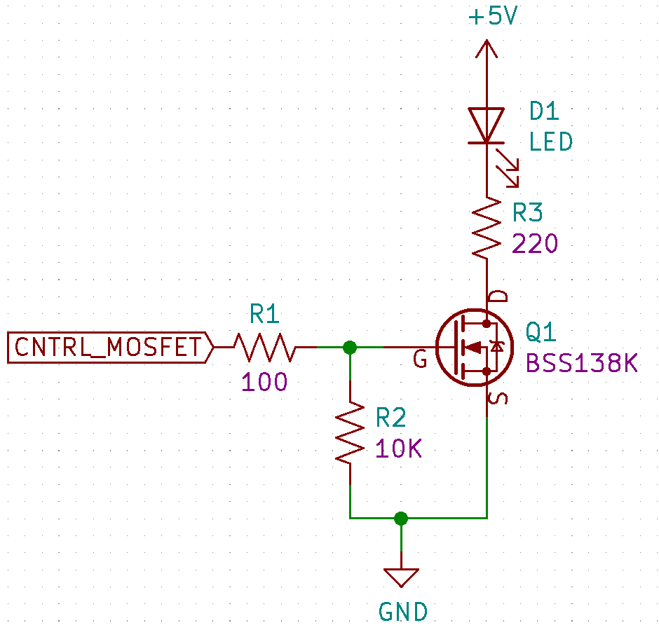
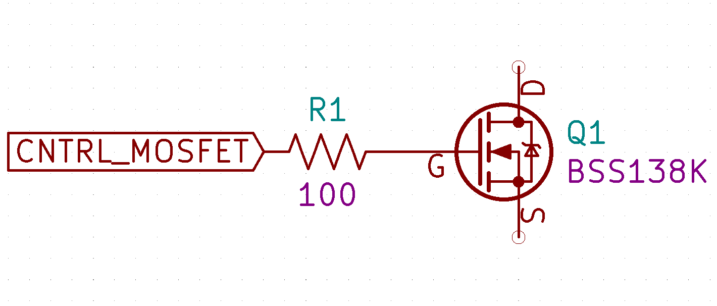
For the rest of this article, I will be limiting the discussion to only discuss N-Channel MOSFETs. These are easier to drive and are the most common type for driving high-power loads. Figure 2 shows the most simplistic MOSFET circuit. R1 is the gate resistor, limiting the amount of current and preventing any ringing on the gate. R2 is a 10K pulldown resistor, ensuring the MOSFET is always in a known state. Q1 is a logic-level MOSFET, an appropriate choice for controlling an indicator LED at 10s of milliamps. Since a Q1 is a logic-level MOSFET, CNTRL_MOSFET can be from the I/O line of a standard microcontroller
“Normal” MOSFET Circuits
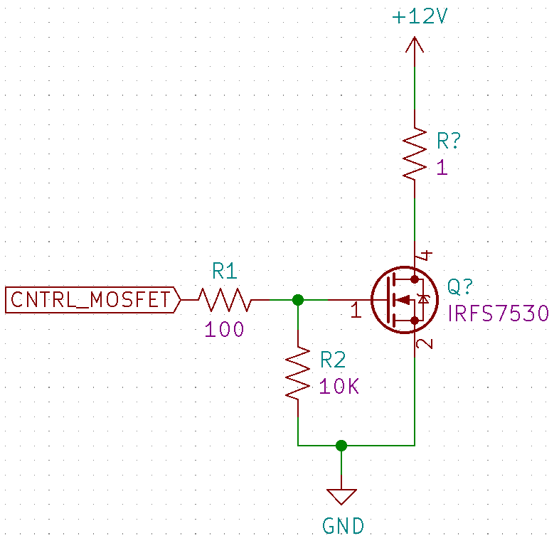
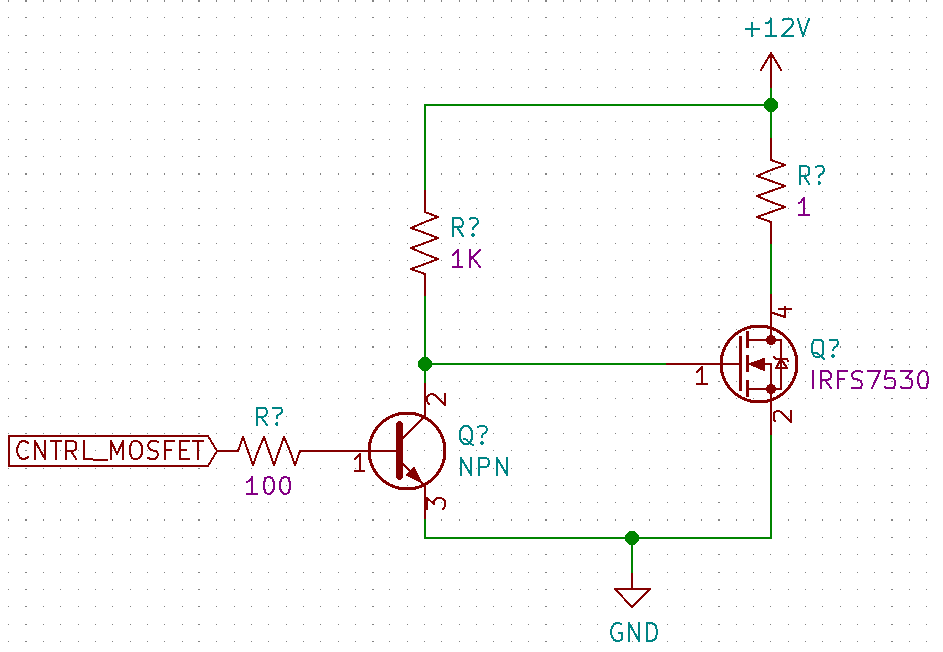
Driving “normal” MOSFETs are slightly more complicated since they need to have at least 10V on the gate to fully conduct. Figure 3 shows a useful example of a low-side N-channel MOSFET circuit. A 12A load is switched from an IRFS7530, a high-power D2PAK MOSFET. This is an example of how you could control a resistive heating element. Since the rate that you PWM the resistor is quite low, a 100R resistor is a valid choice.
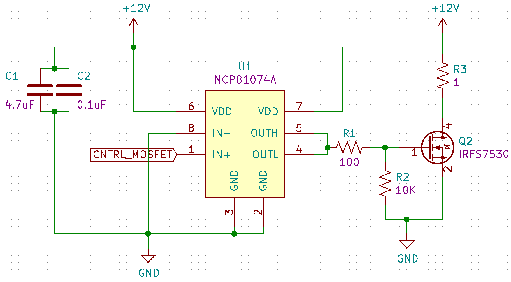
The easiest – and usually best – way to drive power MOSFETs is to use a purpose-built, integrated driver. These chips use internal logic level MOSFET circuitry to take the logic-level input from the microcontroller and switch on/off the MOSFET. Figure 4 shows an NCP81074A based circuit. This is one of my favorite drivers to use, as it has a separate source and sink pin. This allows the switching speed of the on and off times to be fine-tuned if required. Depending on the gate resistor, this chip is able to source 10A to charge the gate incredibly fast, minimizing power losses.
An important item to note is the decoupling capacitors C1/C2. I highly recommend using more capacitance than suggested in the datasheet. Since the driver needs to source a lot of current to turn on the MOSFET, the more capacitance available the better. The length of the traces from pins U1.4/5 to R1 and then Q2.1 should also be as short as possible to minimize the parasitic inductance which would slow the switching speed.
 The only real reason to not use a dedicated gate driver on high-power MOSFETs is to try and minimize cost. A cheaper way to drive a MOSFET is shown in figure 5. I would only recommend this method when absolutely necessary, as dedicated gate drivers are much easier to implement, and tend to have better performance.
Deciphering MOSFET Datasheet Specs
Reading and understanding any component datasheet can be a difficult endeavor, and MOSFETs are no different. Again, my goal with this discussion is not to go down “into the weeds” with equations and derivations. I will discuss good “rules of thumb” for choosing MOSFETs. There are plenty of cases in which you will need to do more in-depth analysis’ and testing to ensure the component chosen will operate correctly.
Let’s say you are designing a custom H-bridge driver for a high powered motor controller. It is a circuit based on 4 power MOSFETs. The specs that this circuit must have are:
- Up to 10A continuous current
- Maximum of 25A stall current
- 12VDC
- “Silent” PWM speed control at an ultrasonic frequency of 20kHz
- Minimize heat dissipation (as always!)
We will use the datasheet from the IRFS7530 MOSFET shown in the previous examples as a reference.
Important Specifications
-
- Id(Package Limited) – This is the maximum theoretical drain current for the package. This is a commonly misunderstood spec by new designers. You absolutely can’t exceed this value, but it does not mean you can actually drive a load at that current. The MOSFET will almost always burn up from heat before this spec is reached. So it must be taken with a grain of salt. The IRFS7530 has an Id of 240A, so we are good there.
- Vgs – Maximum voltage applied to the gate with respect to the source. Pretty self-explanatory. It is +-20V for our MOSFET, and we are using a voltage of 12V, so we are not near the limit.
- Vdss – Another self-explanatory spec. The voltage difference from the drain to the source can’t exceed, which is 60V in this case, well within our safe range.
-
Rds(on) – The maximum expected resistance from drain to source, at a given gate voltage. We find that the MOSFET has a worst-case Rds(on) of 1m4. Figure 6 shows a graph commonly found on MOSFET datasheets. We can see that the Rds(on) flattens out and has it’s the minimum value above ~8V. This is expected from a non-logic-level MOSFET, and acceptable when driven at 12V.
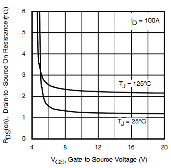
Figure 6: Rds(on) vs Vgs at different temperatures.
- RthetaJA (Junction-to-Ambient) – This is the thermal resistance from the die junction to the outside of the package to ambient air. This will be specified with a specific amount of copper on the PCB.
- Qg – As previously mentioned, this is the total charge required to inject to the gate to fully turn the MOSFET “on”. This takes into account the gate-to-source charge, gate-to-drain-charge, as well as any other internal parasitics. This is the easiest spec to use to calculate the maximum “theoretical” switching speed of the MOSFET.