
Ⅰ. Si family of Power devices
Si Power MOSFET and the SuperJuction Power MOSFET (CoolMOS): High-voltage Si power MOSFETs use a D-MOSFET structure. Key resistances include source contact (RCS), source region (RN+), channel (RCH), accumulation (RA), JFET (RJFET), drift region (RD), N+ substrate (RSUB), and drain contact (RCD). For 1000V Si MOSFETs, RD and RCH dominate, varying with temperature. Their temperature dependency relies on resistivity (ρ) and electron mobility (μ). Channel length (LCH) and cell length (Z) matter. The threshold voltage (Vth) depends on P-region doping (NA), oxide capacitance (Cox), and charge (Qox). Intrinsic carrier concentration (ni) impacts Vth inversely due to its ln-based role. Gate-to-source equivalent impedance includes internal resistance (Rg,int), and gate capacitance involves CGN+ and CGP, tied to N+ and P regions respectively, as shown in Figure 1.
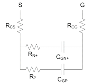
Fig 1 Equivalent impedance circuit of gate to source in Si MOSFET.
On the other hand, the CoolMOS is a device that enhances the planar DMOS structure by introducing a vertical P-N junction. Its higher doping concentration in the drift region compared to conventional power DMOS design, provides a reduced on-state resistance (Rds,on). The resistance components include the source contact, source region, channel, accumulation, drift regions 1 and 2, N+ substrate, and drain contact, while Vth and Rg,int remain akin to Si MOSFET.
Si IGBT: Modern high-voltage Si IGBTs employ a field stop trench-gate structure. The on-state voltage drop comprises VP+N (P+ collector/N-base junction), VNB (N-base region voltage drop considering high-level injection effects), and VMOSFET (MOSFET part voltage drop). Si IGBT shares Si D-MOSFET's Vth and Rg,int, differing in trench gating.
Ⅱ. SiC family of Power devices
• SiC MOSFET: Currently, SiC power devices are primarily made in planar-gate configuration, with a few in trench-gate design. While their Ron and Vth equations resemble Si MOSFETs, they differ in material-related parameters. Notably, SiC MOSFET's channel mobility rises with temperature, unlike Si MOSFET which decreases. Both devices see reduced drain mobility with higher temperatures. Unlike Si, SiC experiences minimal dopant diffusion due to implantation.
• SiC JFET: SiC JFETs now mostly adopt trench-gate designs, differing from SiC MOSFETs. Their Ron lacks accumulation resistance (RA) as in SiC MOSFETs due to their normally-on nature. The channel remains conductive without gate bias. The gate-to-source equivalent impedance includes channel resistance (RCH). Capacitances CP+N- and CN+P+ exist between P+ and N- regions and between P+ and N+ regions, respectively, as illustrated in Figure 2.
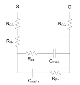
Fig 2 Equivalent impedance circuit of gate to source in SiC MOSFETs.
Ⅲ. Depletion Mode GaN Power Devices and Enhancement Mode GaN Power Devices
Depletion-mode GaN power devices are commonly cascoded with low-voltage Si MOSFETs. Their characteristics, such as Rg,int and Vth, resemble Si MOSFETs. The Ron of GaN HEMTs is described by LD (gate-drain spacing) and ns (2D electron density).
On the other hand, enhancement-mode GaN power devices uses a gate depletion region. This design makes sure that the device remains in an off-state without gate potential, removing the drain-source connection through the 2D electron gas.
Characterization Methods and Results
• Rg,int Characterization: Figure 3 illustrates the overall impedance of vendor C's SiC MOSFET across a 5~100MHz range. It was seen, at 27.5MHz, the impedance curve reflects the series resistance (Rg). Vendor A's Si MOSFET and Si IGBT exhibit temperature-dependent Rg behavior: increasing until approximately 75°C and then decreasing. Meanwhile, vendor D's SiC JFET displays significantly inferior Rg characteristics compared to vendor A's Si MOSFET and Si IGBT. This hinders its viability as a thermal sensing element (TSEP).
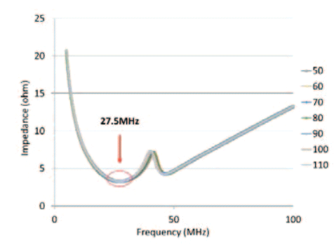
Fig 3 Tj-Impedance relation of SiC MOSFET.
• Onstate Resistance (Ron) Characterization: Figure 4 illustrates that the 1200V Si MOSFET has the highest Ron at 80 ohms, while the other 6 devices exhibit Ron below 1 ohm. Among these, the 650V CoolMOS has the greatest Ron, whereas the 650V eGaN HEMT boasts the smallest. CoolMOS exhibits the highest Tj coefficient at 0.6 ohms/°C, while GaN HEMT cascode shows the lowest at 0.2 ohms/°C. Also, the Tj coefficient range for Ron across all devices was seen to be around 0.4~0.6 ohms/°C.
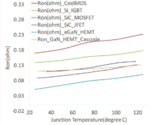
Fig 4 6 devices under different Tj and their Ron.
• Threshold Voltage (Vth) Characterization: The threshold voltage (Vth) assessment was conducted on various devices except for the SiC JFET, which remains normally on. In this evaluation, the gate and drain were shorted. Figure 5 illustrates a close-up of the Ids-Vgs curve for Vth measurement of the GaN HEMT Cascode. Among Wide Bandgap (WBG) devices, the SiC MOSFET exhibited the lowest Vth, approximately 11.2V. The tested eGaN HEMT followed closely, displaying a temperature-dependent fluctuation, unsuitable for TSEP. Another 100V eGaN HEMT from the same manufacturer with a linear Tj coefficient yielded a Vth of 2.22.4V for the GaN HEMT Cascode, primarily dictated by the low voltage Si MOSFET.
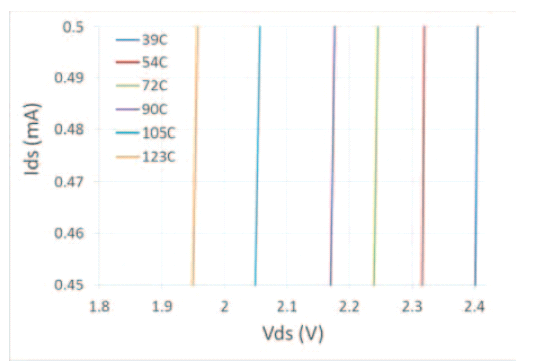
Fig 5 Characterized Ids-Vds curve for measuring Vth.
Ⅳ. Conclusion
An experiment was done to study three TSEPs – internal gate resistance (Rg,int), on-state resistance (Ron), and threshold voltage (Vth) – in different Si, SiC, and GaN power devices.
Ron and Vth exhibited more favourable temperature coefficients for Wide Band Gap (WBG) devices compared to Si. However, using them as TSEPs for WBG applications requires enhanced sensing technology and higher sampling rates due to faster switching. Temperature coefficients of Rg,int varied significantly among manufacturers and proved relevant for only a few devices, warranting careful consideration in its application.