
Analog vs. Digital PDN Impedance and Bandwidth
The primary difference between PDN impedance behavior in analog and digital systems is bandwidth. The bandwidth of a digital signal spans from the switching frequency to the knee frequency, which is equal to approximately 0.35 divided by the signal rise time. The PDN needs to be designed such that the PDN impedance is as low as possible throughout this bandwidth. This requires providing sufficient interplane capacitance, sizing decoupling capacitors correctly, and designing PDN resonances with sufficient damping such that each resonance has low Q-values.
In contrast, the bandwidth of analog signals is very thin. As an example, radar systems have bandwidths that span a few GHz, which is quite small compared to the bandwidth of digital signals. This actually makes analog PDN design much easier as you are only concerned with working in a particular frequency range.
In both types of design problems, you still need to worry about the Q-values of PDN resonances within the relevant bandwidth. The goal is to prevent strong ripple on the power rails and in the power plane. Keeping PDN impedance at all relevant frequencies below some target impedance value is only part of the story; the values of peak resonances and the Q-factor of these resonances is also important. Your PDN should be designed to have the following characteristics:
- Ripple is within tolerances. There will always be some ripple on the output from a PDN. The key is to keep ripple within an acceptable tolerance. In low-level systems, this tolerance may be only a few percent of the supply voltage.
- PDN impedance resonance peaks well below the target impedance. Even if the PDN impedance spectrum is well below the target impedance value, the sum of peak impedances within the relevant bandwidth can still be larger than the target impedance value. This would cause a complicated ripple pattern to have larger peak current and voltage fluctuations than your power budget allows, effectively causing the system to fail.
- For analog signals, no resonances within the bandwidth. In a digital system, you will always have some resonances in the signal bandwidth; the bandwidth of digital signals is simply too large to avoid this. However, analog signal bandwidths are only a small fraction of the carrier signal frequency. Therefore, your carrier signal frequency and bandwidth should not overlap with any resonances in the PDN.
Keeping ripple low in both types of systems is critical for suppressing jitter (in digital systems) or phase noise (in analog systems, the two effects are analogues of each other). Taken together, stackup design and using the right decoupling capacitors will help keep ripple below the target value within the relevant frequency bandwidth. This now becomes a problem of designing the resonances in the PDN impedance spectrum to have low Q-values within the relevant bandwidth.
The figure below shows an example that compares the portions of the PDN impedance spectrum seen by a digital signal with 1 MHz switching frequency and ~25 GHz knee frequency. A high frequency analog signal with low bandwidth is shown for comparison. In this figure, the target PDN impedance is 0.3 milliOhms. Here, the digital signal will see two high Q-factor resonances in the PDN, each of which has 0.2 milliOhms peak impedance. The total impedance from these two resonances is 0.4 milliOhms, which is above the target impedance. A strong ripple pattern will be created by these two resonances when a digital component switches.
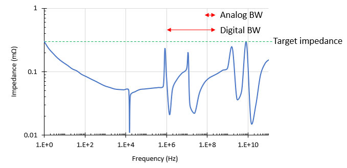
Here, the digital signal bandwidth overlaps with two PDN impedance resonances with high Q-factors. In contrast, the analog signal lies in a flat region of the PDN impedance spectrum where there are no resonances. The analog signal will not produce strong transients, while the digital signal will produce transients that will exceed tolerance levels.
In contrast, the analog signal sits within a relatively flat region of the PDN impedance spectrum. Note that the PDN impedance is not really flat, but the impedance within the analog signal bandwidth is well below the target PDN impedance value. In this case, any transients produced by this example analog component will not exceed the ripple tolerance values.
Designing PDN Impedance for Analog and Digital Signals
As a designer, your job is to precisely engineer the PDN impedance to accommodate the bandwidth of the current being drawn by a component. The current will have frequency components that span over some bandwidth, which generally spans out to infinity. With digital signals, simply take the knee frequency as the upper limit of the bandwidth. With analog signals, such as modulated signals or finite pulses, you can consider a very narrow frequency range when designing the PDN.
Modeling can be very helpful here as long as you include the interplane capacitance, ESL, and ESR values in your circuit simulations. For digital signals, the goal is to create a PDN impedance spectrum that is as flat as possible within the relevant bandwidth. This can be done iteratively by first choosing two decoupling capacitors with high ESR values. One should have a high self-resonance frequency (above the band edge for the signal being drawn), and the other should have a self-resonance frequency that is quite low. As long as the ESR values for these capacitors are large enough, the impedance spectrum for each component will overlap in the PDN, producing a relatively flat spectrum. The ESL values in these capacitors to account for the self-resonance frequencies, and the capacitances will provide sufficient charge to compensate transients.
In a future article, I'll look at this as an optimization problem and show how these component values can be chosen to minimize impedance below some target value. For now, you'll need to simulate the voltage on the PDN for a given current draw and PDN impedance. As you tailor your PDN impedance, and if you know the waveform that will be drawn by a component on the PDN, then you can easily calculate the voltage on the PDN using an inverse Fourier transform. If you think of the PDN impedance as a filter that acts a known current draw, the voltage on the PDN would be calculated with the following equation:

Voltage on a PDN as a function of the current draw and PDN impedance.
Here, the current draw term could be a delta function (for a harmonic current draw), a sawtooth wave, square wave, or any other arbitrary current drawn by a component. Note that the current must be modeled as a causal input signal.
The Remaining Challenge: Accounting for Parasitics
While you can certainly model decoupling capacitors and interplane capacitance in a circuit simulation, it is nearly impossible to account for parasitics exactly without making many loose approximations. Perhaps the greatest challenge is in determining the inductance throughout the PDN as this will determine the Q-factor of each resonance in the PDN.
The image below shows how parasitic inductance throughout a real layout will affect the real inductance seen by transient currents on a PDN. The overally damping is inversely proportional to the PDN inductance. A real layout creates multiple current loops, each of which has their own inductance. This increases the inductance near decoupling capacitors, the inductance created by the plane arrangement, and the total inductance of the PDN. This need to reduce PDN inductance is one reason why decoupling capacitors are normally placed very close to each other and to the output from a VRM.

If you look through a real layout, parasitics create a problem where it is difficult to minimize inductance and sufficiently damp PDN resonances.
Clearly, there is a balancing act that needs to be accomplished. You need to have low inductance in different portions of the circuit, especially near decoupling capacitors, in order to keep damping and capacitor self-resonance frequencies high. However, increasing the inductance in a certain portion of the PDN is useful as this can be used to move a resonance away from the relevant signal bandwidth. This is one reason why decoupling capacitors with high ESR values are often used in high speed digital systems. The high ESR value will provide more damping, which reduces the Q-factor of a particular PDN resonance.