Analog to digital converter (ADC)
Definition of ADC
In the instrumentation system, it is often necessary to convert the detected continuously changing analog quantities such as temperature, pressure, flow rate, speed, light intensity, etc. into discrete digital quantities before inputting them into the computer for processing. These analog quantities are converted into electrical signals (usually voltage signals) by sensors, and after being amplified by amplifiers, they need to undergo certain processing to become digital quantities. A device that converts analog to digital is usually called an analog-to-digital converter (ADC), or A/D for short.
Working principle of ADC
Under normal circumstances, A/D conversion generally needs to go through four processes of sampling, holding, quantization and encoding.
Sampling and holding
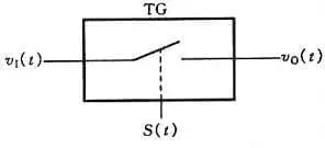
Sampling is to convert an analog quantity that changes continuously with time into a time-discrete analog quantity. The schematic diagram of the sampling process is shown in Figure 1. Figure (a) is a sampling circuit structure, in which the transmission gate is controlled by the sampling signal S(t), during the pulse width τ of S(t), the transmission gate is turned on, the output signal vO(t) is the input signal v1, and During (Ts-τ), the transmission gate is closed and the output signal vO(t)=0. The signal waveforms in the circuit are shown in Figure (b).
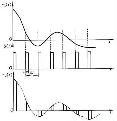
It can be seen from the analysis that the higher the frequency of the sampling signal S(t), the more faithfully the obtained signal can reproduce the input signal after passing through the low-pass filter. But the problem is that the amount of data increases. In order to ensure an appropriate sampling frequency, it must satisfy the sampling theorem.
Sampling theorem: Suppose the frequency of the sampling signal S(t) is fs, and the frequency of the highest frequency component of the input analog signal v1(t) is fimax, then fs and fimax must satisfy the following relationship fs≥2fimax, and fs> is generally taken in engineering (3~5) fimax.
It takes a certain amount of time to convert the analog signal obtained by the sampling circuit into a digital signal each time. In order to provide a stable value for the subsequent quantization and encoding process, the analog signal obtained each time must be held for a period of time by the holding circuit.
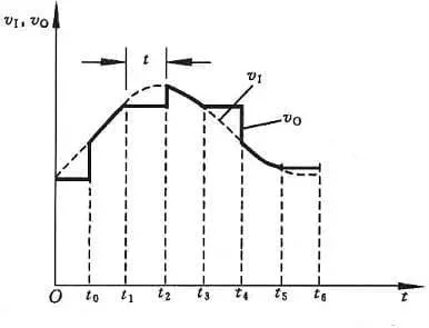
The sampling and holding process is often completed simultaneously through the sampling-holding circuit. The schematic diagram and output waveform of the sample-hold circuit are shown in Figure 2.
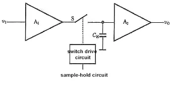
The circuit is composed of input amplifier A1, output amplifier A2, holding capacitor CH and switch drive circuit. A1 is required to have a high input impedance in the circuit to reduce the influence on the input signal source. In order to make it difficult to discharge the charge stored on CH during the holding phase, A2 should also have a high input impedance, and A2 should also have a low output impedance, which can improve the load carrying capacity of the circuit. Generally, it is also required that AV1·AV2=1 in the circuit.
Now in conjunction with Figure 2 to analyze the sample – hold the working principle of the circuit. At t=t0, the switch S is closed, and the capacitor is charged rapidly. Since AV1 · AV2=1, v0=vI, the sampling period is during the time interval of t0~t1. At time t=t1 S is disconnected. If the input impedance of A2 is infinite and S is an ideal switch, it can be considered that the capacitor CH has no discharge circuit, and the voltage at both ends of it remains constant at v0. The flat section from t1 to t2 in Figure 11.8.2(b) is the holding stage.
The sample-hold circuit can be produced by various types of monolithic integrated circuits. For example, there are AD585 and AD684 for bipolar technology; AD1154 and SHC76 for mixed technology.
Quantization and coding
Digital signals are not only discrete in time, but also discontinuous in amplitude. The size of any digital quantity can only be an integer multiple of a specified minimum quantity unit. In order to convert the analog signal into a digital quantity, in the A/D conversion process, the output voltage of the sample-hold circuit must also be normalized to the corresponding discrete level in a certain approximate way. This conversion process is called numerical value. Quantification, referred to as quantification. The quantized value finally needs to be represented by a code through the encoding process. The code obtained after encoding is the digital quantity output by the A/D converter.
The smallest quantity unit taken in the quantization process is called the quantization unit, represented by △. It is the analog quantity corresponding to when the lowest bit of the digital signal is 1, that is, 1LSB.
In the process of quantization, since the sampling voltage is not necessarily divisible by △, there is inevitably an error before and after quantization. This error is called quantization error and is represented by ε. Quantization error is a principle error, which cannot be eliminated. The more bits the A/D converter has, the smaller the difference between discrete levels and the smaller the quantization error.
Two approximate quantization methods are often used in the quantization process: only round-off quantization and round-off quantization.
only rounding up the quantization method
Taking the 3-bit A/D converter as an example, let the input signal v1 range from 0 to 8V. When using the round-up quantization method, take △=1V, and discard the part that is not enough in the quantization unit. If the value is between 0 and 8V The analog voltage between 1V is regarded as 0△, represented by binary number 000, and the analog voltage between 1V and 2V is regarded as 1△, represented by binary number 001… The maximum error of this quantization method is △.
rounding quantization method
If the rounding quantization method is adopted, the quantization unit △=8V/15 is used, and the part less than half the quantization unit will be discarded during the quantization process, and the part equal to or greater than half the quantization unit will be treated as one quantization unit. It treats the analog voltage between 0 ~ 8V/15 as 0△, represented by binary 000, and the analog voltage between 8V/15 ~ 24V/15 is regarded as 1△, represented by binary number 001 means wait.
Comparison
The maximum quantization error│εmax│=1LSB in the former quantization method with rounding only, and the quantization method│εmax│=1LSB/2 in the latter quantization method with rounding and rounding, the quantization error of the latter is smaller than the former, so it is majority A /D converter used.
With the rapid development of integrated circuits, new design ideas and manufacturing techniques for A/D converters emerge in an endless stream. A/D converters with different structures and performances are designed to meet various detection and control needs.
Types of ADC
Integrating ADC
conversion principle
The conversion principle of integrating ADC is based on integrating the voltage and comparing the integrated voltage with another voltage to control the count, and the count output is the ADC output. The object of integration is either based on the reference voltage, or based on the reference voltage and the input voltage.
Pros and Cons
Advantages:
- The integral ADC has high resolution, and the number of digits can be 12 or even higher.
- Linearity is very good. Essentially, the input is compared to an integrated reference voltage to determine the output, so linearity will depend on the accuracy of the comparator.
- The circuit realization topology is simple, and there are relatively few components used to realize these devices, so the circuit is relatively simple and the production cost is low.
Shortcoming:
- The main disadvantage is the slow conversion speed. N-bit ADC, the output may take up to 2 N clock cycles to convert a single sample point.
Applications
Primarily used in sensor applications and devices such as voltmeters and ammeters where accuracy is more important than speed. In other words, the sampling speed of the integral ADC is relatively low, but the accuracy is very high.
classification
There are different types of integral ADCs, and the common ones are single and double slope integrals. Adding a “slope” increases precision at the expense of conversion time.
single slope integral ADC
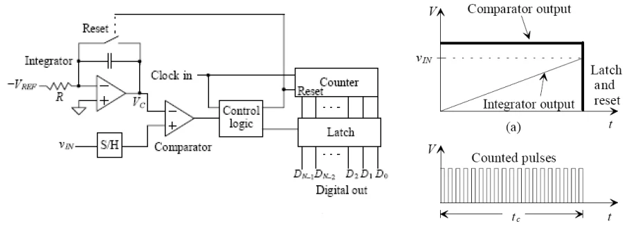
The comparator compares the input voltage to the value of the integrated reference voltage (note that we’ll make it negative since it’s connected to the inverting input of the op amp ). Simultaneously count the number of clock cycles. When the integrator output is equal , the comparator outputs a logic “0”, triggering a reset of the counter and integrator, and the latch holds the digital output.
VINVREFVrefVrefVin
This is the conversion time. I know why this integral ADC is slow. Let’s look at the worst case, assuming the input voltage , assuming , assuming it is a 20-bit ADC, then!
VIN=VREFTCLK=1ustc=220us=1048576us
single slope integral ADC

A dual-slope ADC differs from a single-slope ADC in that the comparison to ground is now made and two sums of voltages are integrated . Initially, the negative input is connected to the integrator, which ramps up until the counter overflows. Since integrating at the inverting input switches to a negative value, the integrator output will always be positive and greater than zero, so the counter will keep running until it overflows, which takes 2N clock cycles (=T1).
VCVREFVINVC

At T2 time, it will be equal to the sum of and, and it
VC=VC1+VC2=0
But:
VIN/VREF=T2/T1
Therefore, the principle of ADC conversion, dual-slope ADC is slower than single-slope ADC, since the integration is performed twice, the error related to the slope of the integrator will be canceled, thus improving the accuracy in principle.
Sigma-Delta Σ-Δ ADC
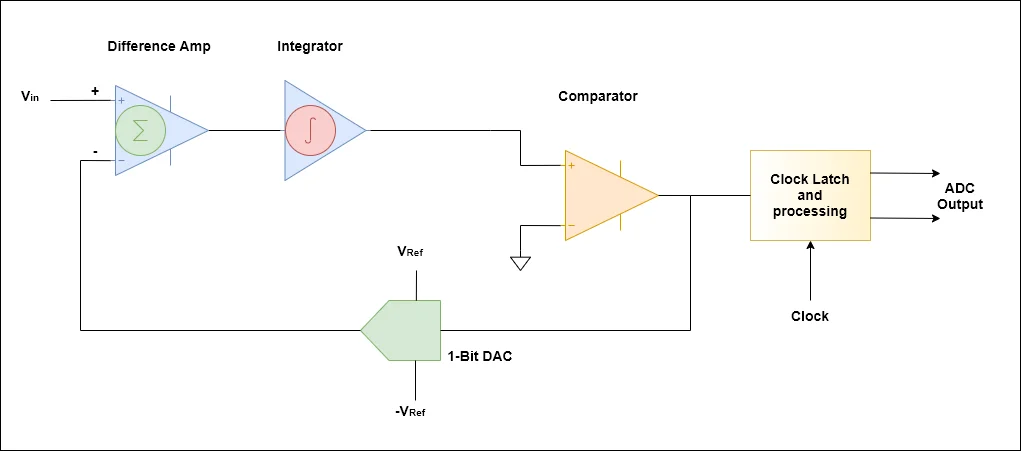
Starting at the input, the difference amplifier produces an output that is the difference between Vin and the 1-bit DAC output. The output of a 1-bit DAC can be one of two values: OR . In this topology, an integrator can be thought of as taking a moving average of the previous value and the current input value.
–Vref+Vref
Therefore, assuming that the comparator positive segment is initially fixed at a small value above 0V, the comparator reverses. Its value will be high or 1. Then, the DAC output will be . On the next iteration, this value will be subtracted from the current value of . Since the previous value was 0V, the integrator output will now be – Vref. At this point, the comparator output will be 0 and the DAC output will be.
+VrefVin-Vref
On the next sample , the integrator output will be 0 due to the previous value, and the difference amplifier will actually subtract , thus adding to . The comparator output will be 1.
-Vref-Vref+VrefVin
This process continues iteratively so, for a 0V input, the comparator output will be a steady stream of 101010…. Remember that logic 1 means , logic 0 means , so if N samples are sampled and averaged, it is easy to see that the average value is 0V. The processing block after the comparator will simply output this as a single value 0000…, assuming a reference value of ( ~ ) or 2 x.
+Vref-Vref-Vref+VrefVref
Now, assuming 1V, this is a 5V ADC. is ±2.5V. Following the same steps as before iteratively, the output will be: 1011101… The output is 1.07V.
Vin±Vref
In summary:
A sigma-delta ADC oversamples the signal being processed (see How Analog-to-Digital Sampling for this concept) and low-pass filters the signal to be processed. Usually, the number of bits converted using the Flash ADC after the filter is less than the required number of bits. The resulting signal, along with errors from the FLASH discrete levels, is fed back and subtracted from the input and fed to the filter. This negative feedback dampens the noise so that it does not appear at the desired signal frequency. A digital filter after the ADC (using a decimation filter) reduces the sampling rate, filters out unwanted noise signals and increases output resolution (hence the name sigma-delta modulation, also known as delta-sigma modulation).
Flash ADC (direct comparison type)
The principle of FLASH ADC may be the easiest to understand. The figure below is a schematic diagram of a two-bit ADC, which consists of many comparators, each of which is provided with a reference voltage that is one bit higher than the previous reference value. Therefore, for an 8-bit ADC, 256 such comparators are required. For 10 bits, you need 1024.
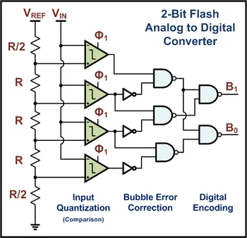
LASH ADC (direct comparison type) is fast. It directly converts the input without any sampling or heavy post-processing. The problem is, it requires a lot of comparators, and a lot of comparators take up a lot of silicon space on the chip. Therefore, use Fash ADCs only when you need extremely high speeds that cannot be achieved with other ADC implementations.
Dichotomy embodied in hardware
In practical applications, there is another variant that is more commonly used, the semi-FLASH ADC. It uses a two-step process to reduce the number of converters needed in the actual conversion chain:
First, the input signal is compared to the set of levels that lie exactly in half . If it is lower, then the most significant bit, MSB, is set to 0 and the input is fed to a chain of comparators with the reference voltage set to convert the rest of the bits.
If the input signal is above , set the MSB to 1, subtract from the input signal . The comparator chain is used again to get the remaining bits. So, in essence, the half-step FLASH ADC sacrifices an extra comparison to save half the comparator. This kind of thinking can also continue to be deduced and expanded, such as 4-point FLASH ADC and so on
The successive approximation register (SAR)
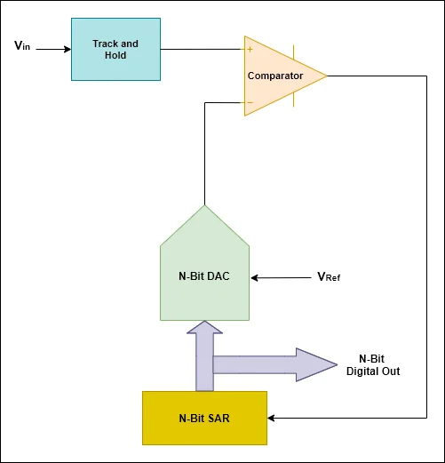
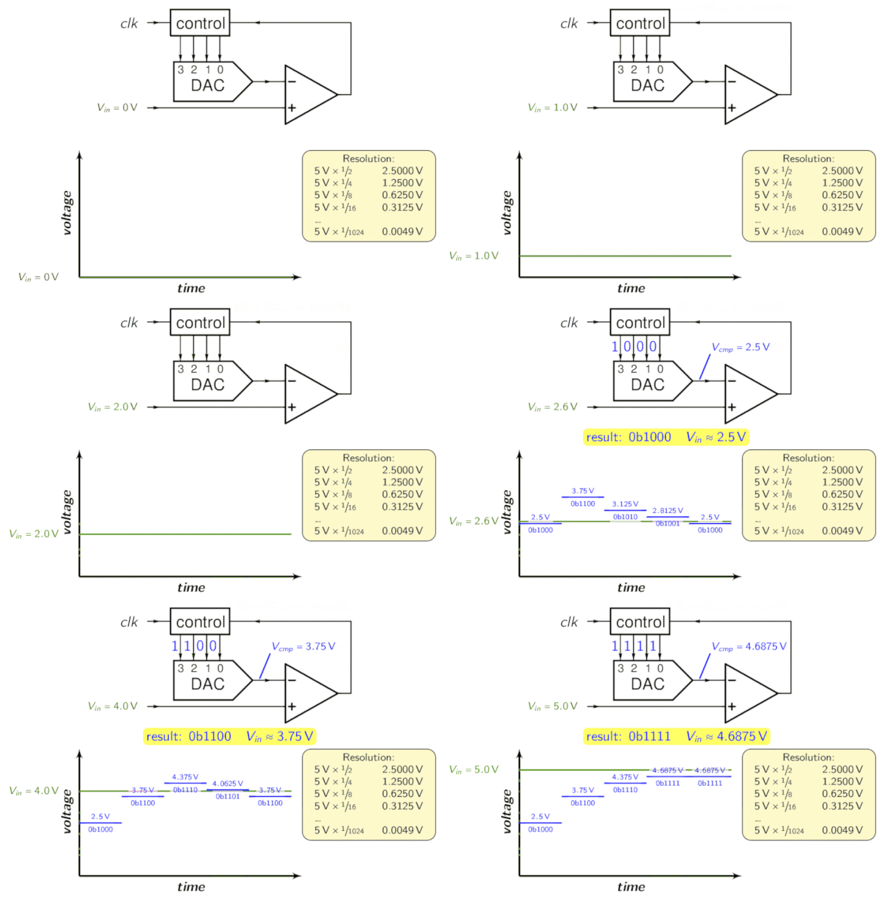
The Successive Approximation Register (SAR) is an integral part of the successive approximation ADC. It works by utilizing a comparator to gradually narrow down the area containing the input voltage. To do this, the converter contrasts the input voltage to the output of a digital-to-analog converter, which usually indicates the middle of the chosen voltage range. With each step of the process, the estimation is stored in the SAR.
For example, suppose the input voltage is 6.3 V and the initial range is 0 to 16v.
- For the first step, input 6.3 V to compare with 8v (the midpoint of the 0-16V range). The comparator reports an input voltage of less than 8v, so the SAR is updated to reduce the range to 0 – 8v.
- In the second step, the input voltage is compared to 4v (the midpoint of 0 – 8v), the comparator reports that the input voltage is above 4v, so the SAR is updated to reflect that the input voltage is in the 4 – 8v range.
- In the third step, the input voltage is compared to 6v (half of 4v to 8v); the comparator reports an input voltage greater than 6 volts, and the search range becomes 6 – 8 volts.
Continue these steps until you reach the desired solution. Its topology is as follows:
For intuition, look at the following animation:
Pipelined ADC
A pipelined ADC (also known as a subroutine quantizer) uses two or more pipelines. First, do a rough conversion. In the second step, a digital-to-analog converter (DAC) is used to determine the difference in the input signal. This difference is then converted into finer values and the results are combined in a final step. This can be considered an improvement over subsequent approximation ADCs, where the feedback reference signal consists of intermediate transitions over the entire range of bits (eg, 4 bits), rather than just the next most significant bit. Combining the advantages of successive approximation method and flash ADC, this type has the advantages of high speed, high resolution and small mold size.
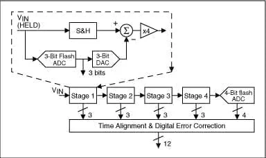
In this schematic, the analog input VIN is first sampled and held steady by a sample-and-hold (S&H), while the flash ADC in the first stage quantizes it to three bits. The 3-bit output is then fed to a 3-bit DAC (12-bit accurate) and the analog output is subtracted from the input. This “remainder” is enlarged by a factor of 4 and sent to the next stage (stage 2). This added remainder continues through the lower stages of the pipeline, providing 3 bits per stage, until it reaches the 4-bit flash ADC, which will resolve the final 4LSB bits. Because the bits for each stage are determined at different points in time, all bits corresponding to the same sample are time aligned with the shift register before being fed to the digital error correction logic. Note that when a pipeline has finished processing input samples, determining the acquisition bit for this pipeline and passing the residual to the next pipeline, it can start processing the next sample received from the sample-holder embedded in each pipeline . This pipelining is the reason for the high throughput, which is also the concept of pipelining.
Others
In addition to the above several common ADCs, there are also charge balance principle ADCs, time-sharing ADCs, FM ADCs, time-stretching ADCs, incremental encoding ADCs, Wilkinson ADCs, etc.
Digital to Analog Converter (DAC)
Definition of DAC
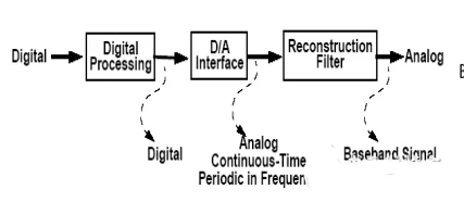
The digital quantity processed by the digital system is sometimes required to be converted into an analog quantity for practical use. This conversion is called “digital-to-analog conversion”. The circuit that completes the digital-to-analog conversion is called a digital-to-analog converter, or DAC (Digital to Analog Converter) for short.
DAC parameters
Resolution
The resolution in DAC is defined as the number of all possible output analog levels under different input digital code values. N-bit resolution means that DAC can generate 2 N −1 different analog levels. Generally, it It refers to the number of digits of the input digital code.
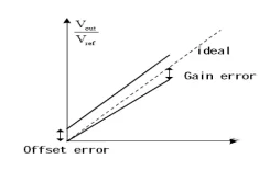
Offset and gain errors
Offset is defined as the value of the actual output analog signal when a code value of 0 is input, and gain error is defined as the difference between the ideal full-scale output value and the actual output value after deducting the offset, as shown in the figure.
Accuracy
The precision in DAC is divided into absolute precision and relative precision. Absolute accuracy is defined as the difference between the ideal output and the actual output, including various offset and non-linear errors. Relative accuracy is defined as the maximum integral nonlinear error. Accuracy is expressed as a ratio of full scale, expressed in effective digits. For example, 8-bit accuracy means that the error of the DAC is less than 1/8 2 of the full-scale output of the DAC. Note that the concept of precision is not related to resolution. A 12-bit resolution DAC may have only 10-bit precision; and a 10-bit resolution DAC may have 12-bit precision. Accuracy over resolution means that the DAC’s transmission response can be controlled more precisely.
INL-Integral Nonlinearity
When offset and gain errors are removed, integral linearity error is defined as the deviation of the actual output transfer characteristic from the ideal transfer characteristic (a straight line). as the picture shows.
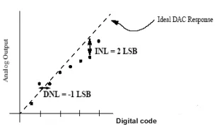
DNL-Differential Nonlinearity
In an ideal DAC with a minimum of 1 LSB per analog output change, differential linearity error is defined as the deviation from 1 LSB per minimum analog output change (excluding gain error and offset). The DNL we define is for each digital input code value, and sometimes the largest DNL is used to define the DNL of the entire DAC. An ideal DAC would have zero differential linearity error for each digital input, while a DAC with a maximum DNL of 0.5LSB would have a minimum output change between 0.5LSB and 1.5LSB per output. The integral and differential linearity errors of the DAC are shown in the figure.
Jitter energy (Glitch Impulse Area)
The maximum area under the jitter that appears at the output after the input signal changes.
Settling Time
The settling time is within a specific error range of the final value, and the time required for the output to experience full-scale conversion.
Monotonicity A monotonic DAC is one in which the output analog level always increases as the input digital code value increases. If the maximum DNL is controlled within 0.5LSB, then the monotonicity of the DAC can be guaranteed naturally.
Spurious Dynamic Range (SFDR) SFDR is Spurious Free Dynamic Range, that is, the dynamic range without noise and harmonics. Both noise and harmonics are called spurious signals.
Principle of DAC
Convert each input binary code into a corresponding analog quantity according to its weight, and then add the analog quantities representing each bit, the total analog quantity obtained is proportional to the digital quantity, thus realizing the conversion from digital quantity to digital quantity Analog conversion.

It is the decimal value converted into a binary number by bit weight expansion.
DAC composition and characteristics
DAC is mainly composed of digital registers, analog electronic switches, bit weight network, summing operational amplifier and reference voltage source (or constant current source). Use the digits of the digital quantities stored in the digital register to control the analog electronic switches of the corresponding digits respectively, so that the digit with a digit of 1 generates a current value proportional to its digit weight on the digit weight network, and then the operational amplifier controls each current value summed and converted to a voltage value.
Varying bit weight networks enable the assembly of multiple kinds of DACs, including the weight resistance network DAC, the R-2R inverted T-shaped resistance network DAC and the single value current type network DAC, etc. The precision of the conversion produced by the weighted resistor network DAC is contingent upon the accuracy of the reference voltage VREF, as well as the quality of the analog electronic switches, operational amplifiers, and weighted resistor values. Its disadvantage is that the resistance values of each weight resistor are different, and when there are many digits, the resistance values vary greatly, which brings great difficulties to ensure the accuracy, especially for the production of integrated circuits. Therefore, in the integrated DAC This circuit is rarely used alone.
Main technical indicators of DAC
Conversion accuracy and conversion speed of DAC: Conversion accuracy is generally described by resolution and conversion error in DAC.
Resolution
Generally, the number of bits of the DAC is used to measure the resolution, because the more the number of bits, the more values (2n) of the output voltage vO, and the more it can reflect the subtle changes of the output voltage. the higher.
In addition, the resolution can also be defined by the ratio of the minimum output voltage 1 LSB that the DAC can distinguish to the maximum output voltage FSR. which is:
resolution=1LSB/FSR=k/k(2n-1)=1/(2n-1)
The smaller the value, the higher the resolution.
Conversion error
Conversion error is the maximum deviation between the actual output analog voltage and the ideal value. Commonly expressed as a percentage or several LSBs of the ratio of this maximum deviation to the FSR. In fact, it is a comprehensive indicator of the three errors.
Conversion speed
Conversion speed is generally determined by the settling time. From when the input changes from all 0s to all 1s, until the output voltage stabilizes within the range of FSR±½ LSB (or the range specified by FSR±x%FSR), this period is called the settling time, which is the maximum response of the DAC Time, so use it to measure the speed of conversion.
Types of DAC
Resistance type
The structure is shown in Figure 1. What Fig. 1 shows is a R-2R ladder network type converter. Its advantage is that it can achieve very good linearity. Since all current sources are equivalent, we can use special additional technology to make the error between them smaller, and its structure is much simpler than that of resistor divider. The disadvantage is that the resistance is always nonlinear, and it also contains parasitic capacitance related to the signal, so it is difficult to achieve complete matching. At the same time, the speed is limited by the output buffer, and the speed cannot be very high.
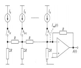
Capacitive type
The structure is shown in Figure 2. The highest-order capacitance CN is 1 2N− times that of the lowest-order capacitance C1. The advantage is that the power consumption is small, and the matching accuracy is higher than that of the resistor. The main limiting factors are the mismatch of capacitors, the on-resistance of the switches, large RC delays, and the impact of the limited bandwidth of the amplifier on the speed of the DAC. A major disadvantage of charge-distributing DACs is that capacitors in CMOS processes take up a lot of chip area to implement. Finally, since the capacitance in the CMOS process is nonlinear in nature, the linearity of the overall DAC will be suppressed. Suitable for medium and wideband high precision.
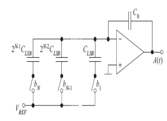
Current type
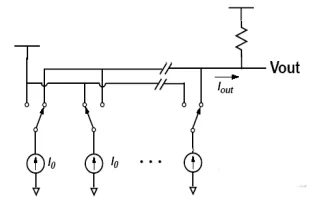
The structure is shown in Figure 3. The advantage is that when the accuracy is less than 10 bits, the area can be made very small, and the speed is not limited by the bandwidth of the amplifier and the large RC delay. It can reach a very high speed. Since all the current flows directly to the output terminal, the energy consumption It is highly efficient and easy to implement. The disadvantages are sensitivity to device mismatch and limited current source output impedance. Suitable for high-speed broadband requirements.
It is also possible not to use an operational amplifier for output, and directly use the load resistance to convert the current into a voltage output, as shown in Figure 4. This form allows the rate of the DAC not to be limited by the bandwidth of the op amp.
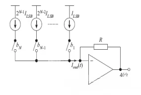
Multiplication type
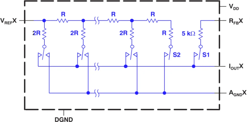
Some of the DA converters use a constant reference voltage, and some add an AC signal to the reference voltage input. The latter is called a multiplication type DA converter because it can obtain the result of multiplying the digital input and the reference voltage input. In general, a multiplying DA converter can not only perform multiplication, but also be used as an attenuator for digitally attenuating an input signal and a modulator for modulating an input signal.
One DA converter
As opposed to the conversion system just talked about, a DA converter uses a special method of transforming digital values into a pulse width modulation or frequency modulation, which then gets smoothed out with a digital filter to produce a commonly used voltage output (also known as bit stream mode) for audio, etc.
