
1. What is a switching power supply snubber circuit?
Snubber circuit is also called absorption circuit, which is an important protection circuit for power electronic devices. It is composed of inductors, capacitors, resistors, power switches and other components, which can protect the normal operation of the circuit. There are many forms of snubber circuits that can be divided into multiple categories according to different classification standards to adapt to different types of switching power supplies.
According to the moment of action of the snubber circuit, it can be divided into turn-off snubber circuit and turn-on snubber circuit. The turn-off snubber circuit can absorb turn-off overvoltage or commutation overvoltage to reduce turn-off power loss, while the turn-on snubber circuit is used to suppress the current when the switching power supply is turned on. If the two snubber circuits are combined, it will form Composite snubber circuit.
Passive and active snubber circuits are classified according to component types. Active snubber circuits contain more components and their structure is relatively complex. The passive buffer circuit has no control and drive circuit, and has a simpler structure and is widely used.
From the perspective of whether the snubber circuit generates loss, it can be divided into lossy circuits and lossless circuits.. There are many classifications of snubber circuits, and the actual use needs to be determined.
1.1 The necessity and function of switching power supply snubber circuit
In order to avoid this situation, we can start from two aspects. One method is to reduce the parasitic capacitance in the switching converter. Another method is to add a snubber circuit in the circuit to slow down the current or voltage to reduce the damage caused by the overheating of the switching power supply. Compared with the former method, adding a snubber circuit is more economical and feasible. The function of the snubber circuit is achieved by improving the switching trajectory of the power semiconductor device. It can suppress the over-voltage and over-current of the switching power supply, reduce the loss of the switching power supply and ensure the safe and reliable operation of the switching power supply.
1.2 The basic idea of designing switching power supply snubber circuit
There are many design forms of switching power supply snubber circuits, but the basic idea is to try to make the anode current of the switching power supply slowly rise when turning on, and the anode voltage slowly rises when turning off, reducing the power loss during the switching process, Therefore, it is avoided that the switchable thyristor is simultaneously subjected to the influence of overcurrent and overvoltage during the conduction and blocking process of the thyristor, resulting in excessive heating of the device and ultimately damage.
The snubber circuit can suppress the rate of increase of the current by using the characteristic that the inductor current cannot change suddenly, So as to achieve the purpose of slowly rising the anode current of the switching power supply when the device is turned on. The characteristic that the capacitor voltage cannot change suddenly is used to control the rising rate of the device voltage, so as to achieve the purpose of slowly rising the anode voltage when the device is turned off.
2.The type of switching power supply snubber circuit
2.1 RCD snubber circuit
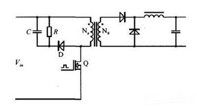
The RCD snubber circuit is composed of a resistor (Rs), a capacitor (Cs) and a diode (VDs). The resistor (Rs) and the diode (VDs) can be connected in series or in parallel. Its main function is to suppress the overvoltage generated when the device is turned off, and to limit du/dt to reduce the turn-off loss of the device.
When the RCD snubber circuit turns off the switching power supply, the load current will shunt when passing through the resistor (Rs) and the capacitor (Cs), reducing the current in the circuit. In addition, the energy stored in the parasitic inductance can be charged by the parasitic capacitance in the switching power supply, so that the switching voltage rises slowly. When the voltage across the parasitic inductance and the parasitic capacitance is the same, the absorption diode VDs will be turned on, so that the switching voltage remains at about one volt.
At the same time, the parasitic inductance can also charge the capacitor, so that when the switch is turned on, it can absorb the capacitor to charge the resistor Rs. The resistor Rs plays a role in suppressing the discharge current. After a period of time, the voltage across the capacitor is close to zero, ready for the switching off of the power supply. The RCD snubber circuit can reduce the voltage stress in the switching power supply to achieve the purpose of protecting the circuit. It is the snubber circuit with the simplest structure and lowest cost, so it is widely used. However, the clamping voltage of this snubber circuit will change with the change of the circuit load. If the parameters of the snubber are unreasonably determined, the snubber circuit will not achieve the desired effect and the switching power supply will be destroyed. In addition, the loss of the RCD snubber circuit is relatively large, which affects the application effect of the circuit.
2.2 LCD snubber circuit

LCD snubber circuit is composed of inductor Lr, capacitor Cs, Cr and diode VD1, VD2, VD3. Since the LCD snubber circuit does not use active devices, and does not contain energy-consuming components, it means that it almost generates no loss, so it is also called a passive lossless snubber circuit.
The function of the LCD buffer circuit is to reduce the rise rate of the current and voltage of the main switch tube, start from zero, make the switch tube work in quasi-zero current conduction and quasi-zero voltage off state, and reduce the loss during the switch on and off. There are many commonly used methods for LCD snubber circuits. One is to connect the inductor in series with the switching tube, so that when the switching power supply is turned on, the current in the loop can only increase from zero, So as to achieve the purpose of protecting the circuit and reducing loss. The capacitor can also be connected in parallel with the switch tube, so that when the power supply is switched, the voltage across the switch tube can only rise slowly from zero, so that the circuit cannot immediately generate overvoltage when it is turned off, so as to achieve the buffering effect. The structure of the LCD snubber circuit is as simple as the RCD snubber circuit, but it has more advantages than the RCD snubber circuit. Its buffering efficiency is very high, the electromagnetic interference to the circuit is small, along with the low cost, good performance and high reliability.
2.3 Energy regenerative snubber circuit

The absorbed energy of the energy regenerative snubber circuit can be directly or indirectly feed back to the DC power supply and load without any controllable switching devices and related control circuits. It has the function of controlling and improving the operation trajectory of the switching device so that it is located in the forward and reverse safe working area, reducing the switching loss and electromagnetic noise of the power device, and improving the overcurrent and overvoltage capability of the device. When the switching power supply is turned on, the parasitic capacitance (Cs) can be discharged through the diode, the transmission capacitance (Co), and the switch absorption inductance resonance circuit. Part of the energy on Cs can be fed back to the switching power supply through diodes, transformers, etc., so as to reduce the peak resonant current and play a role in protecting the circuit. When the switching power supply is disconnected, most of the energy in the inductor Ls can be transferred to the capacitor, and only a small part is fed back to the power supply. So there will be no large surge voltage appear on the switch tube, and it is effectively clamped to reduce the stress of the switch tube. Although the structure of the energy regenerative snubber circuit is more complicated, it can ensure the stable and efficient operation of high-power equipment more than other snubber circuits.
Conclusion
With the development of power electronics technology, switching power supplies are tending to be smaller and lighter. And add a snubber circuit to the circuit can reduce the power burden during the switching of the device. The snubber circuit has now become an indispensable part of the circuit and plays a vital role.