
1. Compare your PCB Design With the Set Standards
PCB designing is a complicated task. It takes years of knowledge and technical experience to be a good PCB Designer. With several possible error zones- it makes sense to follow the regulations. Tally your PCB Designs with the ERC and the DRC constraints. They stand for Electrical Rules Check and the Design Rules Check.
Use them to get parameters for gap widths, trace widths, physical manufacturing requirements. You can also check for performance speed, electrical requirements, or other possible regulations.
Check whether the functionalities of your PCB design meets the required goal. It can help you design a high-quality PCB.
(ALT- Follow the ERC and the DRC)
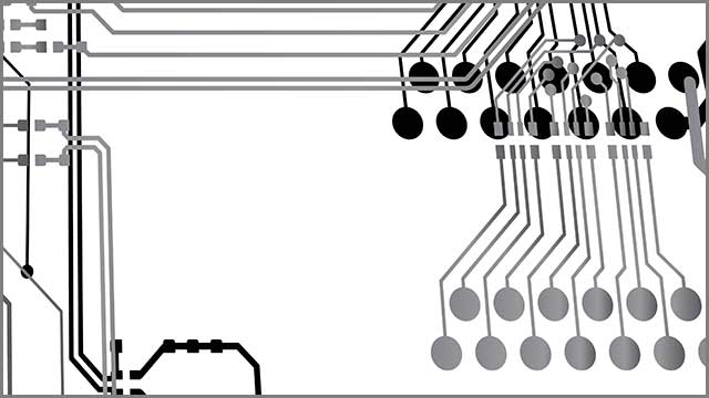
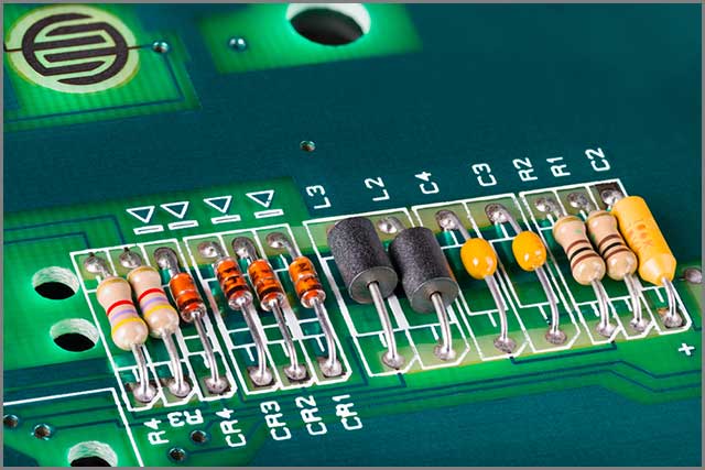
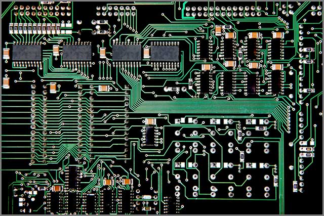
2. Inspect Traces in your PCB Design
Traces are wire conductors responsible for current flow from one component to another. In your PCB- the solder masks cover up the particles. A good practice to reduce errors is color-coding the masks. Traces of only the top and bottom layers of your PCB designs are visible. The usual solder mask color is green- although other colors are also available. White is difficult to notice.
Errors due to Trace misplacement are common. The usual golden rule is- Keep the trace connections as clean as possible. Traces with sharp bends can be problematic for higher power or frequency transmission. Try to avoid steep 90-degree angles. There are exceptions to this general rule too. PCBs with square concentric spirals are a perfect example. We can find these characteristics of high-quality PCB.
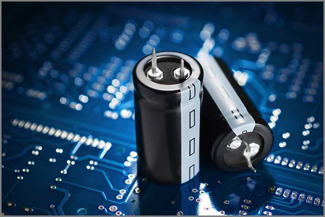
3. Watch out for the Correct Placement of Decoupling Capacitors
Power is essential for each PCB component chip. Traces/Power planes connect components that are at a distance from the power supply.
Decoupling capacitors prevent the harmful effects of high-frequency noise.
Place them close to the chip’s power pins.
A chip with more than one VDD pin needs at least one decoupling capacitor per pin. The reason for such placement- they need to decouple for functioning. The efficiency of the decoupling capacitors decreases if not kept near to the power pins. Your PCB design may be inaccurate if misplaced capacitors are present.
Look out for a new PCB Designer if the present person fails to position the capacitors. It is a grave issue, and mistakes can render the entire PCB making process useless. These will hinder our production of high-quality PCB.
(ALT-high-quality PCB Capacitor Placement is crucial)
4.Quality PCB Trace Length
Analyze the length of your PCB traces. For time-specific functions dependent on many signals- this is critical. High-speed clock signals, data, and address bus lines use these relative PCB functions. The bus lines connect the microprocessor with RAM.
When checking the PCB quality, we should pay attention to:
The length matching ensures signal transmission through the same delay period. The signals arrive at the same time- passing through delay lines.
Knowledge of the PCB layout and schematics is essential. Learn which signal line needs delay lines- and by how much.
Using vias results in added delays. Try to avoid them. If that is not possible, ensure all time-sensitive traces have an equal number of vias. Using delay lines to compensate for vias’ delays is also an option.
(ALT- Match Trace Lengths for Time Functions)
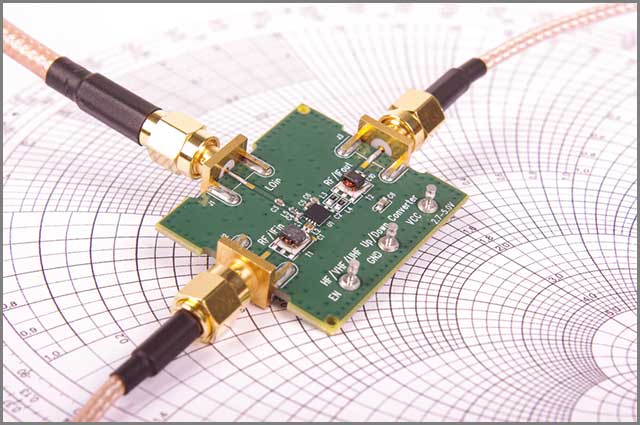
5. Always Match the Impedance in your PCB Designs
Impedance-matching is crucial for all PCB designs. Check whether your design has provisions for receiving and transmitting radio waves. An antenna is also necessary.
For best results, match impedance at all levels. Match the impedance of the feedline between the RF pin to the one connecting it. Match both of these with the antenna impedance. It helps in optimizing the power transmission.
Impedance mismatch decreases power transmission and thereby reduces the device’s operating range. Get controlled impedance by calculating the trace width over the grounded plane. Check the copper trace thickness, dielectric constant, dielectric thickness.
(ALT- Impedance matching is a must for Radio Functions.)
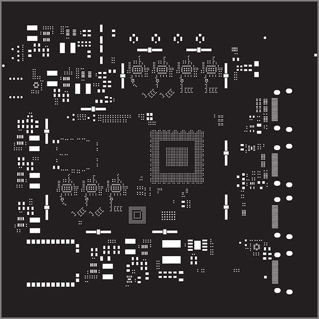
6.High-quality PCB Component Placement
The component placement has a direct effect on your Printed Circuit Board performance. Expert professionals use a generalized series of considerations that help in PCB Designing.
There must be a distance between the inductors in your circuit board. These components create magnetic fields which may result in their coupling, if nearby. Also, avoid placing them near large metallic objects. The output values of the inductor might change. It happens when the magnetic field induces a current in these metal objects.
Adjust if your PCB design consists of power resistors or thermistors. Thermistors and some other components generate significant heat. The heat can affect the performance of the nearby parts.
(ALT- high-quality PCB Right Component Placement improves performance)
7.Confirm that your PCB has Proper Trace Routing and Trace Width
Traces conducting higher amounts of current should have proper routing and width. The primary reason is heat generation due to the current flow. The Printed Circuit Institute (IPC) trace width chart is an excellent reference for finding. When designing your PCB, keep the trace width within the suggested levels.
Traces connecting inductors in your PCB should not exceed the required measurements. Wider bits generated unwanted RF emissions- like antennas. This way, we can ensure PCB quality.
Prevent noise-pickup problems. Avoid placing traces carrying small analog signals parallel to digital signals. The consideration is also valid for fast-changing signs.
(ALT- Avoid Issues of Overheating)
8.Assure Grounding and Ground Planes for Your PCB
The number of layers in your PCB board is dependent on its complexity. PCB boards with a medium level of intricacy should have at least four layers. The inner layers serve as the supply and the ground plane.
Ensure a split Ground Plane for PCB designs consisting of both analog and digital signals. Join the split signals at a common point(with the power supply negative). The digital section of your circuit board generates significant ground current spikes. The splitting prevents the ends from damaging the analog section.
Also, prevent joining any PCB section's ground return paths into a Common Ground Return path. Current flowing the PCB copper traces will cause voltage drops. It will result in different values of ground reference for different compo0nents.
(ALT- Grounding is essential in high-quality PCB, like any other electronic component)
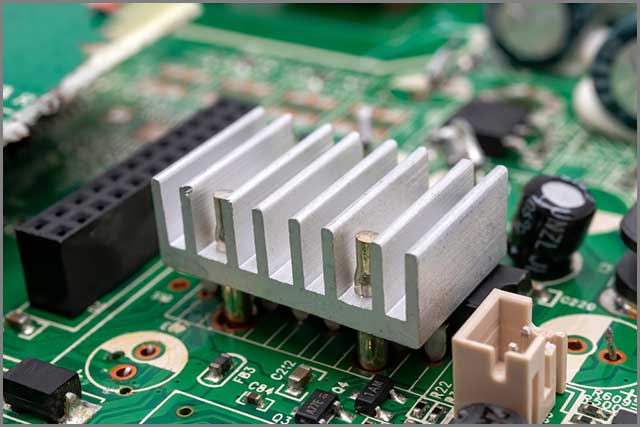
9. Examination of Heat Dissipation Function of High-quality PCB
The Consideration for Heat Dissipation is a must in good PCB Design Practices. List out the PCB components generating the most heat. The next step is planning for steps to dissipate the heat generated. PCB Designer software often has a “Recommended Guidelines” section to help you out.
Keep important PCB components away from high heat-generating sources. Also, heatsinks or cooling fans reduce component temperatures. They might be necessary for your designs.
Thermal Reliefs are useful in wave soldering applications. They slow the heatsinks rate- easing up the soldering process. Also, utilize the ground plane by connecting a via to it. Omitting thermal reliefs on that via will allow heat to transfer onto the ground plane.
(ALT- Consider Heat Dissipation to ensure better performance and longer life)
10.Review the Entire PCB Layout
Make one(or more) final review before sending out the design for manufacture. Reduce the chances of error to the largest extent possible. There are several things to the lookout.
Reviewing your layout can increase your PCB’s performance. Look out for the possible error zones. Check for leakage resistance, interconnecting traces, decoupling, and so on. Irregularities in the trace length or width can turn a capacitor into an inductor.
Organizations often select different people for reviewing of the PCB design. The selection happens based on their specialization. A good understanding of the PCB function is thus necessary. Devote time- do not rush.
(ALT- Review the PCB Layouts to avoid unnecessary costs)