1. Why do we need embedded components?
The traditional method of circuit board design is to place components on the top and bottom surfaces of the circuit board. The patch factory can use special equipment to automatically pick and place to locate each component, and solder the circuit components to the surface through methods such as reflow soldering. Today, the demand for smaller and more integrated electronic products is increasing, and the frequency of circuit signals is increasing, which requires further improvements in manufacturing and assembling circuits.
A technology that can provide higher density and improve high-frequency signals is to embed components into the layers of the circuit structure. For example, embedding discrete components directly under the integrated circuit can shorten the signal length, reduce resistance and parasitic inductance, thereby reducing noise and EMI, and improving the integrity of circuit signals. These improvements provide smaller, more reliable products that support faster signal speeds and higher bandwidth. Combined with the continuous improvement of manufacturing processes and technologies, they can also reduce product size and reduce manufacturing and board-level assembly costs.
In PCB design tools, components can be placed on any signal layer, not just the traditional top or bottom surface signal layer. If they are placed on the internal copper layer, these components are called embedded components.
Embedded components can be divided into two categories: embedded discrete components, such as chip resistors and capacitors, which are then placed on the inner layers of the circuit board during the manufacturing/assembly process; and embedded integrated components formed during the circuit board manufacturing process, that is, components that are actually formed on the inner layers, such as 3M-CPly, etc. PCB design tools support the first type of embedded components, which are then placed on the inner layers of the circuit board during the manufacturing/assembly process.
2. How are devices embedded
The basic way to embed components is to create an open cavity (Cavity) so that the embedded components are located in the cavity. There are two forms of component embedding: semi-embedded, where the cavity remains visible on the finished board; fully embedded, where it is placed on the inner layer and covered with an upper layer during the manufacturing process, making it invisible on the finished substrate.
There are many ways to manufacture PCBs with embedded components, and one process and method is shown below.
1. Start with a double-sided copper-clad core board, and etch and drill each copper layer as needed;
2. Add inner layer Prepreg+Copper, etch and laser drill as needed;
3. Install embedded components using solder and reflow;
4. Add Prepreg, which makes a cutout according to the cavity position;
5. Add outer layer Prepreg+Copper, etch, laser drill and through-hole drill as needed and press fit.

3. Embedded Capacitor Concept
Low voltage and high current have become the trend of power supply design today, and the performance of power supply network (PDN) is increasingly valued by design engineers. With the improvement of the functions of consumer electronic products, more and more devices need to be placed on the limited circuit board area, and the space left for capacitors is getting less and less. In this situation, embedded capacitor design is one of the effective means to improve PDN design.
Embedded capacitors use materials with high capacitance density and reduce the distance between layers to form a large enough inter-plate capacitor as part of the power supply system to achieve decoupling and filtering, thereby reducing the discrete capacitors required on the circuit board and achieving better high-frequency filtering characteristics.
Capacitors made of special materials are placed in the inner layer of the PCB. Because of its very small parasitic inductance, embedded capacitors can effectively reduce the installation inductance of discrete capacitors, which also has a very obvious improvement effect on low frequencies.

4. Classification and specifications of buried capacitors
1. Discrete capacitors are designed to calculate the area of the capacitor according to the required capacitance value in PCB design, and then connected to the power layer in a similar way to the pad when used.
2. Coplanar capacitors do not require special treatment in PCB design. 3. Buried capacitance specifications

Note:
1. BC12TM adds ceramic powder, so Dk increases and buried capacitance density also increases;
2. BC16T only contains resin and adds ceramic powder, the purpose is also to increase Dk and buried capacitance density
V. Technical solutions and implementation methods
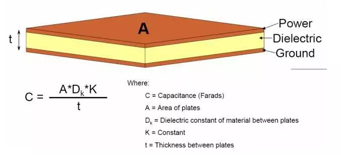
Due to the maturity of processes and technologies, as well as the need for high-speed design for power supply systems, buried capacitance technology is increasingly being used. To use buried capacitance technology, we must first calculate the size of the plate capacitor, the formula is as follows:

Among them:
C is the capacitance of the buried capacitor (plate capacitor)
A is the area of the plate. In most designs, it is difficult to increase the area between the plates when the structure is determined.
Dk is the dielectric constant of the medium between the plates. The capacitance between the plates is proportional to the dielectric constant.
K is the vacuum permittivity, also known as the vacuum permittivity, which is a physical constant with a value of 8.854 187 818×10-12 farad/meter (F/m);
H is the thickness between the planes. The capacitance between the plates is inversely proportional to the thickness. Therefore, if we want to get a larger capacitance, we need to reduce the thickness between the layers. 3M's C-ply buried capacitance material can achieve an interlayer dielectric thickness of 0.56mil, plus a dielectric constant of 16, which greatly increases the capacitance between the plates.
After calculation, 3M's C-ply buried capacitance material can achieve a capacitance between the plates of 6.42nF per square inch.
In a good stack-up, the inter-plate capacitance is normally taken into account. The so-called buried capacitance design is just to use special materials to increase the inter-plate capacitance. For PCB design, it is only necessary to mark the special materials used in addition to the normal stack-up.
