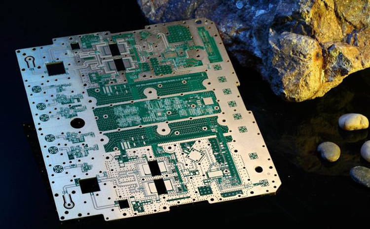
When making high-frequency PCB samples, different surface treatment methods will be used according to the number of layers. For simple single-sided and double-sided boards, most of the surface treatment methods usually use tin spraying or OSP, while high-frequency boards with more than 4 layers use immersion gold surface treatment. Each PCB surface treatment method has its own characteristics. Today, we will introduce several common high-frequency PCB surface treatment methods.

1. Tin spraying
Tin spraying is also called hot air leveling (HASL). In the early days, it was the most commonly used surface treatment method for high-frequency PCB proofing. With the development of PCB, the tin spraying process has become very mature and the cost is low. Now there are lead-free tin spraying and lead tin spraying. Tin spraying is suitable for visual inspection and electrical testing. It is one of the high-quality surface treatment methods in high-frequency PCB proofing.
2. Electroless nickel gold
Electronic nickel gold is also a relatively large PCB surface treatment method in high-frequency PCB proofing. The nickel layer in electroless nickel gold is a nickel-phosphorus alloy layer, which is not explained in detail here. Electroless nickel gold is suitable for lead-free welding, SMT, switch contact design, aluminum wire binding, thick plates, etc. The surface is very flat and has strong resistance to environmental attacks.
3. Nickel palladium gold
Nickel palladium gold was previously used more in semiconductors. With development, it is now gradually applicable to high-frequency PCB proofing. It is cheaper than ENIG and electroless nickel gold, suitable for a variety of surface treatment processes and exists on the board.
4. Electroplating nickel gold
Electroplated nickel gold has hard gold and soft gold. Hard gold is like gold-cobalt alloy, and soft gold is pure gold.
Electroplated nickel gold is more commonly used on IC substrates (such as PBGA), mainly for binding gold wires and copper wires; but when electroplating C substrates, additional conductive wires need to be made at the gold finger binding place before electroplating. In high-frequency PCB proofing, electroplated nickel gold is suitable for contact switch design and gold wire binding, and is suitable for electrical testing.
