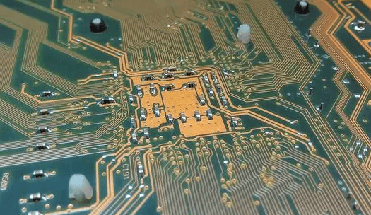
PCB (Printed Circuit Board) and PCBA (Printed Circuit Board Assembly) are indispensable components of electronic devices. They are the physical carriers of electronic components and are responsible for connecting and transmitting electronic signals. Reverse engineering is a technical process of obtaining design information by analyzing and understanding existing products or systems, and then replicating, improving or innovating. In the field of PCB and PCBA, reverse engineering is particularly important, especially in product development, failure analysis, compatibility improvement, etc.
1. What is PCB/PCBA reverse engineering?
PCB/PCBA reverse engineering refers to the analysis of an existing PCB or PCBA to understand its design, structure, and function. This usually involves physical inspection of the circuit board, identification of electronic components, analysis of circuit layout, and simulation of circuit function. The goal of reverse engineering may be to learn design principles, repair faulty equipment, develop compatible products, or upgrade products.
2. PCB/PCBA reverse engineering process
1. Make circuit board pictures
After getting the sample, scan the sample as a whole to obtain the PCBA 3D model and the circuit diagram data of each layer.
2. Make BOM list
Record the model, parameters and position of all components. Especially the direction of diodes and transistors, the direction of IC gaps, and take photos of the positions of the two components with a digital camera to help the subsequent pictures.
3. Retouching
Adjust the contrast and brightness of the canvas to make the copper mold part and the copper mold-free part have a strong contrast. Make sure the transferred image is clear, and then save the picture as a black and white BMP format file TOP BMP and BOT BMP. If you find that there is a problem with the graphics, you can also use PS to modify and modify it.
4. Image calibration
Convert the two BMP format files to PROTEL format files, and transfer the two layers to PROTEL for proofreading. If they cannot overlap well, you need to repeat the third step.
5. Package production
If the component packaging in PROTEL cannot match, we should build the component packaging ourselves.
6. Draw the traces
Convert TOPBMP to TOPP PCB, pay attention to convert to the SILK layer, that is, the yellow layer, and then scan the TOP layer. Place the device according to the drawing in the first step, delete the SILK layer after drawing, and repeat until all layers are drawn.
7. Export PCB file
In PROTEL, call TOPOTEL PCB and BOT PCB into one drawing.
8. Final proofreading
Use a laser printer to print TOPP LAYER BOTTOM LAYER on transparent film respectively, and place the film on the PCB at a ratio of 1:1 to compare whether it is there.
9. Test signal parameter analysis
In this way, the copy board that is the same as the original board is completed, but only half of it is completed. It is necessary to test whether the electronic technical performance of the copy board is the same as the original board.

3. Application of reverse engineering
Product development: By reverse analyzing competitor products, companies can quickly learn and develop their own products.
Fault analysis: When the original design files are lost or incomplete, reverse engineering helps identify and repair faults.
Compatibility improvement: By understanding how existing products work, compatible accessories or upgraded components can be developed.
Education and research: Reverse engineering is an effective way to learn and study the principles of electronic design.
4. Conclusion
PCB/PCBA reverse engineering is a complex but powerful tool that can help companies quickly acquire technical knowledge and improve their competitiveness. However, it also brings legal, technical and cost challenges. The correct use of reverse engineering can promote technological innovation and product improvement under the premise of respecting intellectual property rights.
